- 您現(xiàn)在的位置:買賣IC網(wǎng) > PDF目錄384656 > MAX2450CEP (MAXIM INTEGRATED PRODUCTS INC) 3V, Ultra-Low-Power Quadrature Modulator/Demodulator PDF資料下載
參數(shù)資料
| 型號: | MAX2450CEP |
| 廠商: | MAXIM INTEGRATED PRODUCTS INC |
| 元件分類: | 衰減器 |
| 英文描述: | 3V, Ultra-Low-Power Quadrature Modulator/Demodulator |
| 中文描述: | 70 MHz - 160 MHz RF/MICROWAVE QUADRAPHASE MODEM |
| 文件頁數(shù): | 2/8頁 |
| 文件大小: | 107K |
| 代理商: | MAX2450CEP |
M
3V, Ultra-Low-Power Quadrature
Modulator/Demodulator
2
_______________________________________________________________________________________
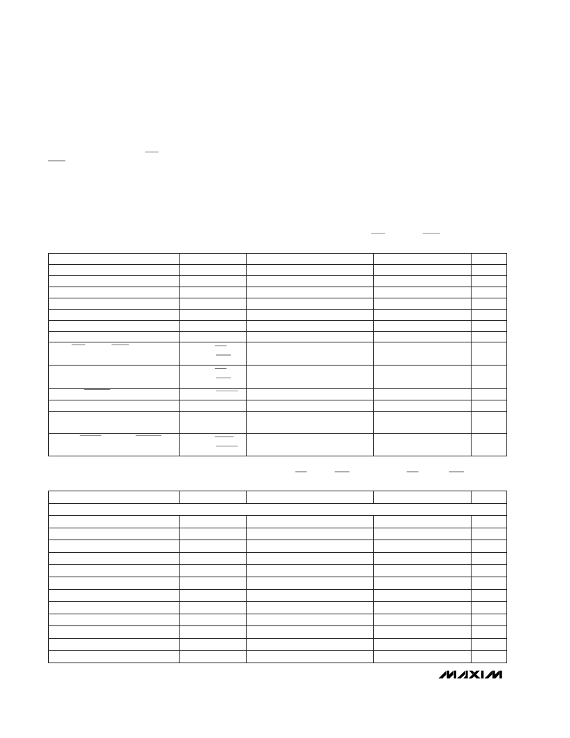
ABSOLUTE MAXIMUM RATINGS
V
CC
, LO_V
CC
to GND............................................-0.3V to +4.5V
ENABLE, TANK,
TANK
, I_IN, I_IN, Q_IN,
Q_IN to GND..................................................-0.3V to (V
CC
+ 0.3V)
IF_IN to GND .........................................................-0.3V to +1.5V
DC ELECTRICAL CHARACTERISTICS
(
V
CC
=
LO
_
V
CC
=
TANK
=
2.7V to 3.3V, ENABLE = V
CC
- 0.4, GND = LO_GND = 0V, I_IN = I_IN = Q_IN = Q_IN = IF_IN = TANK =
OPEN, T
A
= 0°C to +70°C, unless otherwise noted.)
SYMBOL
PARAMETER
Stresses beyond those listed under “Absolute Maximum Ratings” may cause permanent damage to the device. These are stress ratings only, and functional
operation of the device at these or any other conditions beyond those indicated in the operational sections of the specifications is not implied. Exposure to
absolute maximum rating conditions for extended periods may affect device reliability.
Continuous Power Dissipation (T
A
= +70°C)
QSOP (derate 9.1mW/°C above +70°C)......................727mW
Operating Temperature Range...............................0°C to +70°C
Storage Temperature Range.............................-65°C to +165°C
Lead Temperature (soldering, 10sec) .............................+300°C
ENABLE = 0.4V
ENABLE = V
CC
CONDITIONS
V
1.2
V
I_OUT/I_OUT
,
V
Q_OUT/Q_OUT
I_OUT, I_OUT, Q_OUT, Q_OUT
DC Bias Voltage Level
AC ELECTRICAL CHARACTERISTICS
(MAX2450 EV kit, V
CC
= LO_V
CC
= ENABLE = 3.0V, f
LO
= 140MHz, f
I_IN
/
I_IN
= f
Q_IN/Q_IN
= 600kHz, V
I_IN/I_IN
= V
Q_IN/Q_IN
= 1.2Vp-p,
f
IF_IN
= 70.1MHz, V
IF_IN
= 2.82mVp-p, T
A
= +25°C, unless otherwise noted.)
SYMBOL
PARAMETER
DEMODULATOR
μA
μs
μA
V
V
2
20
I
CC(OFF)
t
ON/OFF
I
EN
V
ENH
V
ENL
Shutdown Supply Current
Enable/Disable Time
ENABLE Bias Current
ENABLE High Voltage
ENABLE Low Voltage
mA
5.9
8.2
I
CC(ON)
V
2.7
3.3
V
CC
, LO_V
CC
Supply Voltage Range
Supply Current
320
400
480
Z
IF_IN
Demodulator IF Input Impedance
Demodulator I and Q Baseband
DC Offset
V
V
CC
- 1.5
V
IF_OUT/IF_OUT
IF_OUT, IF_OUT DC Bias Voltage
k
35
44
Z
I_IN/I_IN
,
Z
Q_IN/Q_IN
Modulator Differential Input
Impedance
V
1.25
1.5
1.75
V
I_IN/I_IN
,
V
Q_IN/Q_IN
I_IN, I_IN, Q_IN, Q_IN
Self-Bias DC Voltage Level
10
1
3
V
CC
- 0.4
0.4
UNITS
MIN
TYP
MAX
(Note 2)
(Note 2)
CONDITIONS
dB
< ±0.45
< ±1.3
51
I and Q Amplitude Balance
I and Q Phase Accuracy
Voltage Conversion Gain
Allowable I and Q Voltage Swing
Noise Figure
dBc
MHz
MHz
dBc/Hz
V
p-p
-60
9
IM5
I/Q
BW
DEMOD
f
LO
I and Q IM5 Level
I and Q Signal 3dB Bandwidth
Oscillator Frequency Range
LO Phase Noise
PRE_OUT Output Voltage
dBc
-44
IM3
I/Q
I and Q IM3 Level
degrees
dB
V
p-p
dB
UNITS
MIN
TYP
MAX
R
L
= 10k
, C
L
< 6pF, rising edge
(Notes 1, 3)
10kHz offset
R
L
= 10k
, C
L
< 6pF
V/μs
60
SR
PRE_OUT
PRE_OUT Slew Rate
70
160
-80
0.35
V
PRE_OUT
(Note 1)
1.35
mV
±11
±50
18
NF
相關(guān)PDF資料 |
PDF描述 |
|---|---|
| MAX2451 | 3V, Ultra-Low-Power Quadrature Demodulator |
| MAX2451CSE | 3V, Ultra-Low-Power Quadrature Demodulator |
| MAX2452 | 3V, Ultra-Low-Power Quadrature Modulator |
| MAX2463EAI | 900MHz Image-Reject Transceivers |
| MAX2421EAI | 900MHz Image-Reject Transceivers |
相關(guān)代理商/技術(shù)參數(shù) |
參數(shù)描述 |
|---|---|
| MAX2450CEP+ | 功能描述:調(diào)節(jié)器/解調(diào)器 RoHS:否 制造商:Texas Instruments 封裝 / 箱體:PVQFN-N24 封裝:Reel |
| MAX2450CEP+T | 功能描述:調(diào)節(jié)器/解調(diào)器 RoHS:否 制造商:Texas Instruments 封裝 / 箱體:PVQFN-N24 封裝:Reel |
| MAX2450CEP-T | 功能描述:調(diào)節(jié)器/解調(diào)器 RoHS:否 制造商:Texas Instruments 封裝 / 箱體:PVQFN-N24 封裝:Reel |
| MAX2450CEP-W | 功能描述:調(diào)節(jié)器/解調(diào)器 RoHS:否 制造商:Texas Instruments 封裝 / 箱體:PVQFN-N24 封裝:Reel |
| MAX2450CWP | 功能描述:調(diào)節(jié)器/解調(diào)器 RoHS:否 制造商:Texas Instruments 封裝 / 箱體:PVQFN-N24 封裝:Reel |
發(fā)布緊急采購,3分鐘左右您將得到回復(fù)。