- 您現(xiàn)在的位置:買賣IC網(wǎng) > PDF目錄383343 > MAX1961EEP (MAXIM INTEGRATED PRODUCTS INC) 2.35V to 5.5V, 0.5% Accurate, 1MHz PWM Step-Down Controllers with Voltage Margining PDF資料下載
參數(shù)資料
| 型號: | MAX1961EEP |
| 廠商: | MAXIM INTEGRATED PRODUCTS INC |
| 元件分類: | 穩(wěn)壓器 |
| 英文描述: | 2.35V to 5.5V, 0.5% Accurate, 1MHz PWM Step-Down Controllers with Voltage Margining |
| 中文描述: | SWITCHING CONTROLLER, 1120 kHz SWITCHING FREQ-MAX, PDSO20 |
| 封裝: | QSOP-20 |
| 文件頁數(shù): | 20/29頁 |
| 文件大?。?/td> | 455K |
| 代理商: | MAX1961EEP |
第1頁第2頁第3頁第4頁第5頁第6頁第7頁第8頁第9頁第10頁第11頁第12頁第13頁第14頁第15頁第16頁第17頁第18頁第19頁當(dāng)前第20頁第21頁第22頁第23頁第24頁第25頁第26頁第27頁第28頁第29頁

M
4) The circuit parasitic inductance, L
PAR
, is calculated
by:
5) The resistor for critical dampening, R
SNUB
= 2
π
x
f
R
x L
PAR
. The resistor value can be adjusted up
or down to tailor the desired damping and the
peak voltage excursion.
6) The capacitor, C
SNUB
, should be at least 2 to 4
times the value of the C
PAR
to be effective.
7) The snubber circuit power loss is dissipated in the
resistor, P
RSNUB
, and can be calculated as:
where V
IN
is the input voltage, and f
S
is the
switching frequency. Choose R
SNUB
power rating
that exceeds the calculated power dissipation.
MOSFET Power Dissipation
Worst-case power dissipation occurs at duty factor
extremes. For the high-side MOSFET, the worst-case
power dissipation due to resistance occurs at minimum
input voltage (V
IN(MIN)
):
V
V
IN MIN
(
The following formula calculates switching losses for
the high-side MOSFET, but is only an approximation
and not a substitute for evaluation:
P
D N SWITCHING
(
1
(
where V
IN(MAX)
is the maximum value of the input volt-
age, t
FALL
and t
RISE
are the fall and rise time of the
MOSFET, I
L(PEAK)
and I
L(VALLEY)
are the maximum
peak and valley inductor current, and f
S
is the PWM
switching frequency:
I
L(PEAK)
= I
OUT(MAX)
×
(1 + 0.5
×
LIR) and I
L(VALLEY)
=
I
OUT(MAX)
×
(1 - 0.5
×
LIR)
where LIR is the peak-to-peak inductor ripple current
divided by the load current.
The total power dissipation in the high-side MOSFET is
the sum of these two power losses:
P
D(N1)
= P
D(N1RESISTIVE)
+ P
D(N1SWITCHING)
For the low-side MOSFET, the worst-case power dissi-
pation occurs at maximum input voltage:
Applications Information
PC Board Layout Guidelines
A properly designed PC board layout is important in
any switching DC-DC converter circuit. If possible,
mount the MOSFETs, inductor, input/output capacitors,
and current-sense resistor on the top side. Connect the
ground for these devices close together on a power-
ground trace. Make all other ground connections to a
separate analog ground plane. Connect the analog
ground plane to power ground at a single point.
To help dissipate heat, place high-power components
(MOSFETs, inductor, and current-sense resistor) on a
large PC board area. Keep high-current traces short and
wide to reduce the resistance in these traces. Also make
the gate drive connections (DH and DL) short and wide,
measuring 10 to 20 squares (50mils to 100mils wide if the
MOSFET is 1in from the controller IC).
For the MAX1960/MAX1961, connect LX and PGND to
the low-side MOSFET using Kelvin sense connections.
For the MAX1962, connect CS and OUT to the current-
sense resistor using Kelvin sense connections.
Place the REF capacitor, the BST diode and capacitor,
and the charge-pump components as close as possible
to the IC. If the IC is far from the input capacitors, bypass
V
CC
to GND with a 0.1
μ
F or greater ceramic capacitor
close to the V
CC
pin.
For an example PC board layout, see the MAX1960
evaluation kit.
P
V
V
I
R
D N RESISTIVE
(
2
OUT
IN MAX
(
LOAD
DS ON
(
)
)
)
×
×
2
1
=
-
I
t
I
t
V
f
L PEAK
(
FALL
L VALLEY
(
RISE
IN MAX
(
2
S
)
)
)
)
×
×
)
×
×
=
+
PD
I
R
N RESISTIVE
(
1
OUT
LOAD
DS ON
(
)
)
)
×
×
2
=
P
C
V
f
RSNUB
SNUB
IN
S
(
)
=
L
f
C
PAR
R
PAR
=
×
1
2
(
)
π
2.35V to 5.5V, 0.5% Accurate, 1MHz PWM
Step-Down Controllers with Voltage Margining
20
______________________________________________________________________________________
DL
LX
DH
PGND
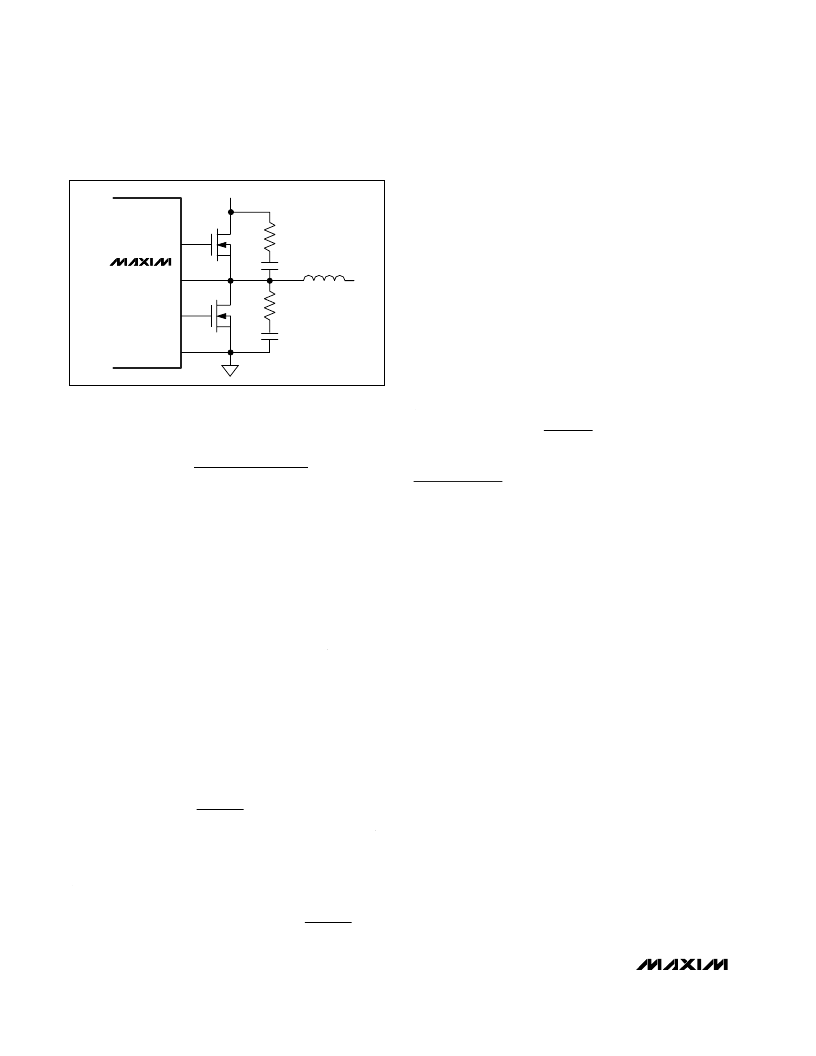
MAX1960
N2
R
SNUB
C
SNUB
C
SNUB
R
SNUB
L1
N1
INPUT
Figure 8. RC Snubber Circuit
相關(guān)PDF資料 |
PDF描述 |
|---|---|
| MAX1960 | 2.35V to 5.5V, 0.5% Accurate, 1MHz PWM Step-Down Controllers with Voltage Margining |
| MAX1960EEP | 2.35V to 5.5V, 0.5% Accurate, 1MHz PWM Step-Down Controllers with Voltage Margining |
| MAX1961 | 2.35V to 5.5V, 0.5% Accurate, 1MHz PWM Step-Down Controllers with Voltage Margining |
| MAX1962 | 2.35V to 5.5V, 0.5% Accurate, 1MHz PWM Step-Down Controllers with Voltage Margining |
| MAX1962EEP | 2.35V to 5.5V, 0.5% Accurate, 1MHz PWM Step-Down Controllers with Voltage Margining |
相關(guān)代理商/技術(shù)參數(shù) |
參數(shù)描述 |
|---|---|
| MAX1961EEP+ | 功能描述:DC/DC 開關(guān)控制器 1MHz PWM Step-Down RoHS:否 制造商:Texas Instruments 輸入電壓:6 V to 100 V 開關(guān)頻率: 輸出電壓:1.215 V to 80 V 輸出電流:3.5 A 輸出端數(shù)量:1 最大工作溫度:+ 125 C 安裝風(fēng)格: 封裝 / 箱體:CPAK |
| MAX1961EEP+T | 功能描述:DC/DC 開關(guān)控制器 1MHz PWM Step-Down RoHS:否 制造商:Texas Instruments 輸入電壓:6 V to 100 V 開關(guān)頻率: 輸出電壓:1.215 V to 80 V 輸出電流:3.5 A 輸出端數(shù)量:1 最大工作溫度:+ 125 C 安裝風(fēng)格: 封裝 / 箱體:CPAK |
| MAX1961EEP-T | 功能描述:DC/DC 開關(guān)控制器 RoHS:否 制造商:Texas Instruments 輸入電壓:6 V to 100 V 開關(guān)頻率: 輸出電壓:1.215 V to 80 V 輸出電流:3.5 A 輸出端數(shù)量:1 最大工作溫度:+ 125 C 安裝風(fēng)格: 封裝 / 箱體:CPAK |
| MAX1962EEP | 功能描述:DC/DC 開關(guān)控制器 RoHS:否 制造商:Texas Instruments 輸入電壓:6 V to 100 V 開關(guān)頻率: 輸出電壓:1.215 V to 80 V 輸出電流:3.5 A 輸出端數(shù)量:1 最大工作溫度:+ 125 C 安裝風(fēng)格: 封裝 / 箱體:CPAK |
| MAX1962EEP+ | 功能描述:DC/DC 開關(guān)控制器 1MHz PWM Step-Down RoHS:否 制造商:Texas Instruments 輸入電壓:6 V to 100 V 開關(guān)頻率: 輸出電壓:1.215 V to 80 V 輸出電流:3.5 A 輸出端數(shù)量:1 最大工作溫度:+ 125 C 安裝風(fēng)格: 封裝 / 箱體:CPAK |
發(fā)布緊急采購,3分鐘左右您將得到回復(fù)。