- 您現(xiàn)在的位置:買賣IC網(wǎng) > PDF目錄383326 > MAX1565ETJ (MAXIM INTEGRATED PRODUCTS INC) Small, High-Efficiency, Five-Channel Digital Still Camera Power Supply PDF資料下載
參數(shù)資料
| 型號(hào): | MAX1565ETJ |
| 廠商: | MAXIM INTEGRATED PRODUCTS INC |
| 元件分類: | 穩(wěn)壓器 |
| 英文描述: | Small, High-Efficiency, Five-Channel Digital Still Camera Power Supply |
| 中文描述: | 3.6 A SWITCHING REGULATOR, 1000 kHz SWITCHING FREQ-MAX, QCC32 |
| 封裝: | 5 X 5 MM, 0.80 MM HEIGHT, MO-220WHHD-2, TQFN-32 |
| 文件頁數(shù): | 22/26頁 |
| 文件大小: | 512K |
| 代理商: | MAX1565ETJ |
第1頁第2頁第3頁第4頁第5頁第6頁第7頁第8頁第9頁第10頁第11頁第12頁第13頁第14頁第15頁第16頁第17頁第18頁第19頁第20頁第21頁當(dāng)前第22頁第23頁第24頁第25頁第26頁

M
SEPIC Buck-Boost
The MAX1565
’
s internal switch step-up and step-down
can be cascaded to make a high-efficiency buck-boost
converter, but it may sometimes be desirable to build a
second buck-boost converter with an AUX_ controller.
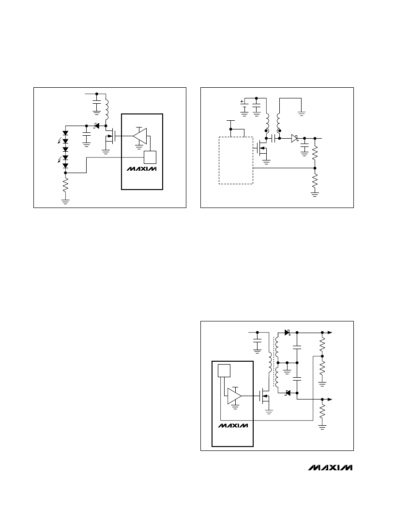
One type of step-up/step-down converter is the SEPIC
(Figure 7). Inductors L1 and L2 can be separate induc-
tors or wound on a single core and coupled like a
transformer. Typically, a coupled inductor improves
efficiency since some power is transferred through the
coupling, causing less power to pass through the cou-
pling capacitor (C2). Likewise, C2 should have low ESR
to improve efficiency. The ripple current rating must be
greater than the larger of the input and output currents.
The MOSFET (Q1) drain-to-source voltage rating, and
the rectifier (D1) reverse-voltage rating must exceed
the sum of the input and output voltages. Other types of
step-up/step-down circuits are a flyback converter and
a step-up converter followed by a linear regulator.
Multiple Output Flyback Circuits
Some applications require multiple voltages from a single
converter channel. This is often the case when generating
voltages for CCD bias or LCD power. Figure 8 shows a
two-output flyback configuration with AUX_. The
controller drives an external MOSFET that switches the
transformer primary. Two transformer secondaries
generate the output voltages. Only one positive output
voltage can be fed back, so the other voltages are set
by the turns ratio of the transformer secondaries. The
load stability of the other secondary voltages depends
on transformer leakage inductance and winding resis-
tance. Voltage regulation is best when the load on the
secondary that is not fed back is small when compared
to the load on the one that is. Regulation also improves
if the load current range is limited. Consult the trans-
former manufacturer for the proper design for a given
application.
Boost with Charge Pump for Positive and
Negative Outputs
Negative output voltages can be produced without a
transformer, using a charge-pump circuit with an auxil-
iary controller as shown in Figure 9. When MOSFET Q1
turns off, the voltage at its drain rises to supply current
to V
OUT
+. At the same time, C1 charges to the voltage
V
OUT
+ through D1.
Small, High-Efficiency, Five-Channel
Digital Still Camera Power Supply
22
______________________________________________________________________________________
MAX1565
(PARTIAL)
AUX_
PWM
OUTSU
DL_
FB_
10
μ
H
TO V
BATT
1
μ
F
1
μ
F
62
(FOR 20mA)
WHITE
LEDs
Figure 6. AUX_ Channel Powering a White LED Step-Up
Current Source
Q
1
C
2
D
1
R
1
OUTPUT
3.3V
L
1
R
2
MAIN
IN
DCON
PART OF
MAX1565
DL
FB
INPUT
1-CELL
Li+
L
2
Figure 7. Auxiliary SEPIC Configuration
MAX1565
(PARTIAL)
AUX_
PWM
OUTSU
DL_
FB_
TO V
BATT
1
μ
F
1
μ
F
1
μ
F
+15V
30mA
CCD+
-7.5V
20mA
CCD-
1.1M
100k
*(SEE NOTE)
*LOAD RESISTOR REQUIRED IF -7.5V
OPERATES WITH NO LOAD
Figure 8. +15V and -7.5V CCD Bias with Transformer
相關(guān)PDF資料 |
PDF描述 |
|---|---|
| MAX1566-MAX1567 | Six-Channel, High-Efficiency, Digital Camera Power Supplies |
| MAX156ACNG | 8-/4-Channel ADCs with Simultaneous T/Hs and Reference |
| MAX156BCNG | 8-/4-Channel ADCs with Simultaneous T/Hs and Reference |
| MAX156BENG | 8-/4-Channel ADCs with Simultaneous T/Hs and Reference |
| MAX155AEPI | 8-/4-Channel ADCs with Simultaneous T/Hs and Reference |
相關(guān)代理商/技術(shù)參數(shù) |
參數(shù)描述 |
|---|---|
| MAX1565ETJ+ | 功能描述:PMIC 解決方案 5Ch Digital Camera Power Supply RoHS:否 制造商:Texas Instruments 安裝風(fēng)格:SMD/SMT 封裝 / 箱體:QFN-24 封裝:Reel |
| MAX1565ETJ+T | 功能描述:PMIC 解決方案 5Ch Digital Camera Power Supply RoHS:否 制造商:Texas Instruments 安裝風(fēng)格:SMD/SMT 封裝 / 箱體:QFN-24 封裝:Reel |
| MAX1565ETJ-T | 功能描述:PMIC 解決方案 5Ch Digital Camera Power Supply RoHS:否 制造商:Texas Instruments 安裝風(fēng)格:SMD/SMT 封裝 / 箱體:QFN-24 封裝:Reel |
| MAX1565EVKIT | 制造商:Maxim Integrated Products 功能描述:SMALL, HIGH-EFFICIENCY, FIVE-CHANNEL DSC - Bulk |
| MAX1566ETL | 功能描述:PMIC 解決方案 RoHS:否 制造商:Texas Instruments 安裝風(fēng)格:SMD/SMT 封裝 / 箱體:QFN-24 封裝:Reel |
發(fā)布緊急采購,3分鐘左右您將得到回復(fù)。