- 您現(xiàn)在的位置:買賣IC網(wǎng) > PDF目錄224149 > M56710FP (Mitsubishi Electric Corporation) F2F MAGNETIC STRIPE ENCORDING CARD READER PDF資料下載
參數(shù)資料
| 型號(hào): | M56710FP |
| 廠商: | Mitsubishi Electric Corporation |
| 英文描述: | F2F MAGNETIC STRIPE ENCORDING CARD READER |
| 中文描述: | F2F磁條讀卡器ENCORDING |
| 文件頁(yè)數(shù): | 1/8頁(yè) |
| 文件大小: | 184K |
| 代理商: | M56710FP |
F2F MAGNETIC STRIPE ENCORDING CARD READER
M56710FP
MITSUBISHI <CONTROL / DRIVER IC>
PIN CONFIGURATION (TOP VIEW)
DESCRIPTION
The M56710FP is a semiconductor integrated circuit of BiCMOS
structure having an F2F demodulator function for magnetic card
reader.
FEATURES
q Low current dissipation (0.7mA when on standby as a standard)
q Provided with glance-over selection input (4, 8, and 16 bits)
q Provided with output polarity (“L” active or “H” active) switching
input
q Miniature mini-mold package
q Wide operating temperature range Ta = -20 – 75
°C
APPLICATION
Magnetic card reader
FUNCTION
Data signal which is read from magnetic card via magnetic head is
input from HD2 and HD1 pins, and converted into F2F pattern
signal by analog processing in amplifier OP1, differentiator OP2,
sensitivity setting circuit and waveform shaping circuit. If F2F signal
is input, the logic section glances over the prescribed number of
bits set by IB1 and IB2 input before performing digital processing,
and then outputs card reading signal CLS, read clock signal RCP,
and read data signal RDT. INV turning to “L” switches each output
of CLS, RCP and RDT from “L” active to “H” active.
STANDARD BITS:
Let the number of glance-over bits set by IB1 and IB2 be M.
Let the Mth FC (flux change) through M+1st FC after LDI input is
turned from “L” to “H” be a standard bit with a time width of TB0.
I/O is discriminated from the next bit to this standard bit as a data
bit.
Outline 20P2N-A
I/O discrimination
Let the data bit time width of a data bit be TBn, and if there is one
next FC between the FC at the end of that bit (i.e. the beginning
of the next bit) to 5/7TBn, let the next bit (Bn+1) be data “1”, and,
if there is no FC, be data “0”.
Output signal time width
When letting the oscillation cycle of oscillation circuit be TOSC,
RCP output pulse width TOW about 16TOSC
RCP delay time to RDT about 8TOSC
20
17
18
19
1
4
3
2
16
5
15
6
14
7
13
8
12
9
11
10
Read control input
F2F output
Noise filter
Differentiator input
Amplifier output
Amplifier (–) input
Amplifier (+) input
Standard voltage
output
Grounding
LDI
NC
F2F
PKO
PKI
AMP
HD2
HD1
VRF
GND
→
←
→
←
→
VCC1
VCC2
CX1
CX2
IB1
IB2
INV
CLS
RDT
RCP
Power supply
Oscillation capacitor
Ignore bit 1
Ignore bit 2
Invert input
Card travelling
signal output
Read data output
Power supply
Read clock output
←
→
M5
6710F
P
NC: no connection
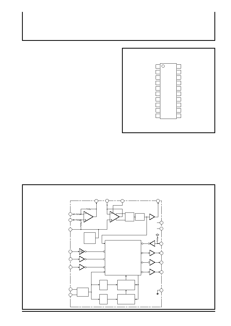
BLOCK DIAGRAM
Card travelling signal output
4
5
6
7
8
9
10
1
15
16
11
12
13
14
3
19
20
17
18
Amplifier
output
PKI
Differentiator
input
AMP
Noise filter
PKO
F2F output
F2F
VCC2
VCC1
INV
CLS
RDT
RCP
GND
11 bit
downcounter
11 bit
upcounter
5TOSC
7TOSC
1/7
1/5
TOSC
Oscillation
circuit
Reference
voltage
circuit
OP1
OP2
Control circuit
Sensitivity
setting
Waveform
shaping
HD2
HD1
Amplifier (-) input
Amplifier (+) input
VRF
Reference voltage output
LDI
Read control input
IB2
Ignore bit 2
IB1
Ignore bit 1
CX2
Oscillation capacitor
CX1
Oscillation capacitor
Power supply
Invert input
Read data output
Read clock output
相關(guān)PDF資料 |
PDF描述 |
|---|---|
| M56733 | 3-PHASE BRUSHLESS MOTOR CONTROL |
| M56733AFP | 3-PHASE BRUSHLESS MOTOR CONTROL |
| M56745FP | SPINDLE MOTOR DRIVER |
| M56748FP | 4-CHANNEL ACTUATOR MOTOR DRIVER |
| M56749 | 4 CHANNEL ACTUATOR MOTOR DRIVER |
相關(guān)代理商/技術(shù)參數(shù) |
參數(shù)描述 |
|---|---|
| M56710FP#TC0J | 制造商:Renesas Electronics Corporation 功能描述: |
| M56710FP(#TC0J) | 制造商:Renesas Electronics Corporation 功能描述: |
| M5671-SL001 | 制造商:Alpha Wire 功能描述: |
| M5671-SL002 | 制造商:Alpha Wire 功能描述: |
| M5671-SL005 | 制造商:Alpha Wire 功能描述: |
發(fā)布緊急采購(gòu),3分鐘左右您將得到回復(fù)。