- 您現(xiàn)在的位置:買賣IC網(wǎng) > PDF目錄370963 > M51996AP (Mitsubishi Electric Corporation) RADIATION HARDENED HIGH EFFICIENCY, 5 AMP SWITCHING REGULATORS PDF資料下載
參數(shù)資料
| 型號(hào): | M51996AP |
| 廠商: | Mitsubishi Electric Corporation |
| 元件分類: | 基準(zhǔn)電壓源/電流源 |
| 英文描述: | RADIATION HARDENED HIGH EFFICIENCY, 5 AMP SWITCHING REGULATORS |
| 中文描述: | 抗輻射高效,5安培開(kāi)關(guān)穩(wěn)壓器 |
| 文件頁(yè)數(shù): | 3/22頁(yè) |
| 文件大小: | 366K |
| 代理商: | M51996AP |
第1頁(yè)第2頁(yè)當(dāng)前第3頁(yè)第4頁(yè)第5頁(yè)第6頁(yè)第7頁(yè)第8頁(yè)第9頁(yè)第10頁(yè)第11頁(yè)第12頁(yè)第13頁(yè)第14頁(yè)第15頁(yè)第16頁(yè)第17頁(yè)第18頁(yè)第19頁(yè)第20頁(yè)第21頁(yè)第22頁(yè)
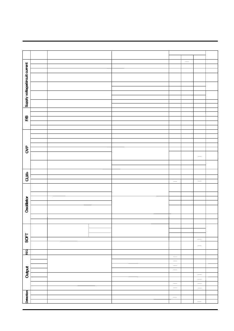
SWITCHING REGULATOR CONTROL
M51996AP/FP
MITSUBISHI (Dig./Ana. INTERFACE)
( 3
Vcc=Vcc
(START) -
Vcc
(STOP)
Operation stop voltage
Stand-by current
Operating supply voltage range
Operation start up voltage
Operating circuit current
Current at 0% duty
Current at maximum duty
Current difference between max and 0% duty
Limits
Typ.
Min.
Max.
30
17.2
10.9
Symbol
Test conditions
Unit
Parameter
ELECTRICAL CHARACTERISTICS
(V
CC
=18V, Ta=25°C, unless otherwise noted)
V
V
Vcc(STOP)
Block
V
CC(START)
V
CC(STOP)
V
CC
I
FBMIND
I
FBMAXD
16.2
9.9
V
9.0
6.3
7.6
100
100
11
12
2.0
210
-1.5
-0.6
-0.99
5.9
600
750
30
150
150
9.0
V
mV
mV
V
dB
μA
μA
V
V
F/B terminal voltage
OVP terminal resistance
OVP terminal H threshold voltage
Difference supply voltage between
operation stop and OVP reset
Current from OVP terminal for
OVP reset
Detection voltage
DET terminal input current
Voltage gain of detection amp
OVP terminal hysteresis voltage
OVP terminal threshold current
OVP terminal input current
OVP reset supply voltage
I
FB
V
FB
R
FB
V
THOVPH
V
THOVP
I
THOVP
I
INOVP
V
CCOVPC
V
CC(STOP)
-
V
CCOVPC
V
DET
I
INDET
G
AVDET
I
THOVPC
mV
μA
ns
V
THCLM+
I
INCLM+
T
PDCLM+
Vcc
Icc
L
Icc
O
Icc
OVP
Vcc
(START)
,Vcc
(STOP)
difference
Circuit current in OVP state
CLM+ terminal threshold voltage
CLM+ terminal current
Delay time from CLM+ to V
OUT
Vcc=14.5V,Ta=25°C
Vcc=14.5V,-30
≤
Ta
≤
85°C
Vcc=15V,f=188kHz
Vcc=30V,f=188kHz
Vcc=25V
Vcc=9.5V
F/B terminal input current
F/B terminal input current
I
FB
=I
FBMIND
-I
FBMAXD
F/B terminal input current=0.95mA
V
μA
μA
mA
mA
mA
μA
mA
μA
mA
15.2
5.0
65
50
7.3
8
1.3
140
-2.1
-0.9
-1.35
4.9
420
540
150
200
17
19
3.0
320
-1.0
-0.4
-0.70
7.1
780
960
100
200
-200
180
-280
220
-140
V
DET
=2.5V
2.4
2.5
1.0
40
2.6
3.0
30
80
80
7.5
250
250
10.0
0.55
1.20
-480
-210
-320
-140
-213
-93
V
THOVP
=V
THOVPH
-V
THOVPL
V
OVP
=400mV
OVP terminal is open.
(high impedance)
Vcc=30V
Vcc=18V
V
CLM
+=0V
Maximum ON duty
Upper limit voltage of oscillation waveform
Lower limit voltage of oscillation waveform
Oscillating frequency
Voltage difference between upper limit and
lower limit of OSC waveform
T-ON terminal voltage
T-OFF terminal voltage
Oscillating frequency during
SOFT operation
SOFT terminal discharging current
Output low voltage
Output high voltage
Output voltage rise time
Output voltage fall time
f
OSC
T
DUTY
V
OSCH
V
OSCL
V
OSC
mA
V
V
V
V
V
V
ns
ns
170
188
207
47
3.97
1.76
50
4.37
1.96
53
4.77
2.16
2.11
2.41
2.71
170
111
19.0
188
131
23.3
207
151
27.0
-0.5
-0.1
1
3.3
0.04
0.7
0.85
1.3
16.7
16.5
60
40
0.4
1.4
1.0
2.0
16.0
15.5
kHz
%
V
kHz
V
V
f
OSCSOFT
I
SOFTIN
V
OL
1
V
OL
2
V
OL
3
V
OL
4
V
OH
1
V
OH
2
T
RISE
T
FALL
V
SOFT
=5.5V
V
SOFT
=2.5V
V
SOFT
=0.2V
R
ON
=20k
,R
OFF
=17k
C
F
=220pF,-5
≤
Ta
≤
85°C
R
ON
=20k
,R
OFF
=17k
C
F
=220pF
V
SOFT
=1V
Discharge current of SOFT terminal at
Vcc less than Vcc
(STOP)
Vcc=18V,Io=10mA
Vcc=18V,Io=100mA
Vcc=5V,Io=1mA
Vcc=5V,Io=100mA
Vcc=18V,Io=-10mA
Vcc=18V,Io=-100mA
V
REG
V
T-ON
V
T-OFF
I
SOFDIS
R
ON
=20k
R
OFF
=17k
R
ON
=20k
,R
OFF
=17k
C
F
=220pF
Regulator output voltage
3.8
2.9
4.5
3.5
5.4
4.2
V
V
μA
6.8
7.8
8.8
V
SOFT terminal input current
相關(guān)PDF資料 |
PDF描述 |
|---|---|
| M51996FP | RADIATION HARDENED HIGH EFFICIENCY, 5 AMP SWITCHING REGULATORS |
| M51997 | RADIATION HARDENED HIGH EFFICIENCY, 5 AMP SWITCHING REGULATORS |
| M51997FP | RADIATION HARDENED HIGH EFFICIENCY, 5 AMP SWITCHING REGULATORS |
| M51997P | RADIATION HARDENED HIGH EFFICIENCY, 5 AMP SWITCHING REGULATORS |
| M52001SP | SYNC SIGNAL PROCESSOR |
相關(guān)代理商/技術(shù)參數(shù) |
參數(shù)描述 |
|---|---|
| M51996AP(#TF0J) | 制造商:Renesas Electronics Corporation 功能描述: |
| M51996FP | 制造商:MITSUBISHI 制造商全稱:Mitsubishi Electric Semiconductor 功能描述:M51996P |
| M51996P | 制造商:MITSUBISHI 制造商全稱:Mitsubishi Electric Semiconductor 功能描述:M51996P |
| M51997 | 制造商:MITSUBISHI 制造商全稱:Mitsubishi Electric Semiconductor 功能描述:SWITCHING REGULATOR CONTROL |
| M51997FP | 制造商:MITSUBISHI 制造商全稱:Mitsubishi Electric Semiconductor 功能描述:SWITCHING REGULATOR CONTROL |
發(fā)布緊急采購(gòu),3分鐘左右您將得到回復(fù)。