- 您現(xiàn)在的位置:買賣IC網(wǎng) > PDF目錄359726 > M38854FD-HP (Renesas Technology Corp.) PLCC Socket; Number of Contacts:32; Terminal Type:PCB Surface Mount; Contact Plating:Tin Over Nickel; Mounting Type:Surface Mount PDF資料下載
參數(shù)資料
| 型號(hào): | M38854FD-HP |
| 廠商: | Renesas Technology Corp. |
| 英文描述: | PLCC Socket; Number of Contacts:32; Terminal Type:PCB Surface Mount; Contact Plating:Tin Over Nickel; Mounting Type:Surface Mount |
| 中文描述: | 單芯片8位CMOS微機(jī) |
| 文件頁數(shù): | 42/103頁 |
| 文件大?。?/td> | 1580K |
| 代理商: | M38854FD-HP |
第1頁第2頁第3頁第4頁第5頁第6頁第7頁第8頁第9頁第10頁第11頁第12頁第13頁第14頁第15頁第16頁第17頁第18頁第19頁第20頁第21頁第22頁第23頁第24頁第25頁第26頁第27頁第28頁第29頁第30頁第31頁第32頁第33頁第34頁第35頁第36頁第37頁第38頁第39頁第40頁第41頁當(dāng)前第42頁第43頁第44頁第45頁第46頁第47頁第48頁第49頁第50頁第51頁第52頁第53頁第54頁第55頁第56頁第57頁第58頁第59頁第60頁第61頁第62頁第63頁第64頁第65頁第66頁第67頁第68頁第69頁第70頁第71頁第72頁第73頁第74頁第75頁第76頁第77頁第78頁第79頁第80頁第81頁第82頁第83頁第84頁第85頁第86頁第87頁第88頁第89頁第90頁第91頁第92頁第93頁第94頁第95頁第96頁第97頁第98頁第99頁第100頁第101頁第102頁第103頁
41
3885 Group
SINGLE-CHIP 8-BIT CMOS MICROCOMPUTER
MITSUBISHI MICROCOMPUTERS
+ 2 cycles (3.375
μ
s)
+ 1 cycle < 4.0
μ
s (3.25
μ
s)
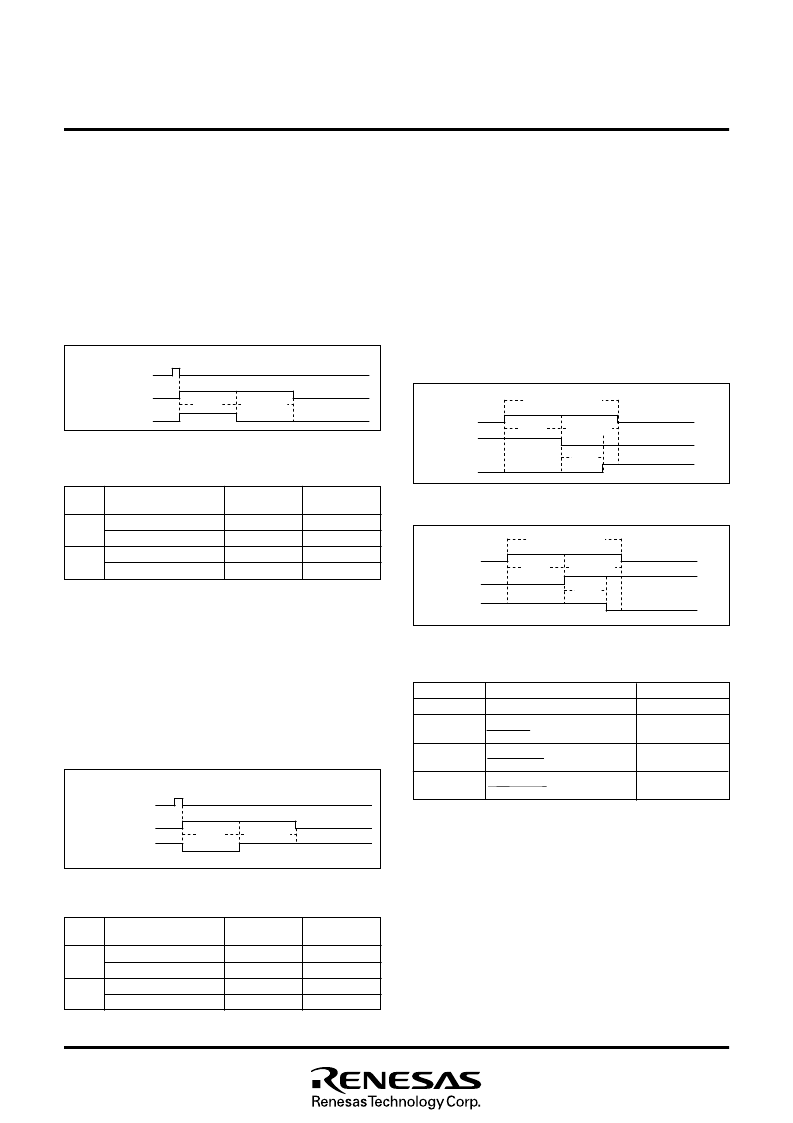
Fig. 39 START condition detecting timing diagram
START/STOP Condition Detecting Operation
The START/STOP condition detection operations are shown in
Figures 39, 40, and Table 14. The START/STOP condition is set
by the START/STOP condition set bit.
The START/STOP condition can be detected only when the input
signal of the S
CL
and S
DA
pins satisfy three conditions: S
CL
re-
lease time, setup time, and hold time (see Table 14).
The BB flag is set to
“
1
”
by detecting the START condition and is
reset to
“
0
”
by detecting the STOP condition.
The BB flag set/reset timing is different in the standard clock mode
and the high-speed clock mode. Refer to Table 14, the BB flag set/
reset time.
Note:
When a STOP condition is detected in the slave mode (MST = 0), an
interrupt request signal
“
I
2
CIRQ
”
occurs to the CPU.
Table 14 START condition/STOP condition detecting conditions
Note:
Unit : Cycle number of system clock
φ
SSC value is the decimal notation value of the START/STOP condi-
tion set bits SSC4 to SSC0. Do not set
“
0
”
or an odd number to SSC
value. The value in parentheses is an example when the I
2
C START/
STOP condition control register is set to
“
18
16
”
at
φ
= 4 MHz.
Fig. 40 STOP condition detecting timing diagram
S
CL
release time
Standard clock mode
SSC value + 1 cycle (6.25
μ
s)
High-speed clock mode
4 cycles (1.0
μ
s)
2 cycles (1.0
μ
s)
2 cycles (0.5
μ
s)
3.5 cycles (0.875
μ
s)
SSC value
2
SSC value
2
SSC value
–
1
2
Setup time
Hold time
BB flag set/
reset time
cycle < 4.0
μ
s (3.0
μ
s)
START Condition Generating Method
When writing
“
1
”
to the MST, TRX, and BB bits of the I
2
C status
register (S1) at the same time after writing the slave address to
the I
2
C data shift register (S0) with the condition in which the ES0
bit of the I
2
C control register (S1D) and the BB flag are
“
0
”
, a
START condition occurs. After that, the bit counter becomes
“
000
2
”
and an S
CL
for 1 byte is output. The START condition gen-
erating timing is different in the standard clock mode and the
high-speed clock mode. Refer to Figure 37, the START condition
generating timing diagram, and Table 12, the START condition
generating timing table.
STOP Condition Generating Method
When the ES0 bit of the I
2
C control register (S1D) is
“
1
”
, write
“
1
”
to the MST and TRX bits, and write
“
0
”
to the BB bit of the I
2
C sta-
tus register (S1) simultaneously. Then a STOP condition occurs.
The STOP condition generating timing is different in the standard
clock mode and the high-speed clock mode. Refer to Figure 38,
the STOP condition generating timing diagram, and Table 13, the
STOP condition generating timing table.
Fig. 37 START condition generating timing diagram
Fig. 38 STOP condition generating timing diagram
Table 13 STOP condition generating timing table
Item
Setup
time
START/STOP condition
generating selection bit
“
0
”
“
1
”
“
0
”
“
1
”
Standard
clock mode
5.5
μ
s (22 cycles)
13.5
μ
s (54 cycles)
5.5
μ
s (22 cycles)
13.5
μ
s (54 cycles)
Note:
Absolute time at
φ
= 4 MHz. The value in parentheses denotes the
number of
φ
cycles.
High-speed
clock mode
3.0
μ
s (12 cycles)
7.0
μ
s (28 cycles)
3.0
μ
s (12 cycles)
7.0
μ
s (28 cycles)
Table 12 START condition generating timing table
Item
Setup
time
START/STOP condition
generating selection bit
“
0
”
“
1
”
“
0
”
“
1
”
Standard
clock mode
5.0
μ
s (20 cycles)
13.0
μ
s (52 cycles)
5.0
μ
s (20 cycles)
13.0
μ
s (52 cycles)
Note:
Absolute time at
φ
= 4 MHz. The value in parentheses denotes the
number of
φ
cycles.
High-speed
clock mode
2.5
μ
s (10 cycles)
6.5
μ
s (26 cycles)
2.5
μ
s (10 cycles)
6.5
μ
s (26 cycles)
Hold
time
Hold
time
I
2
C
w
t
s
e
t
a
s
t
g
u
s
n
r
l
e
g
i
s
t
e
r
r
i
i
a
H
o
l
d
t
i
m
e
Setup
time
S
C
L
S
DA
I
2
C status register
write signal
Hold time
S
e
t
t
u
e
p
i
m
S
CL
S
DA
H
o
l
d
t
i
m
e
Setup
time
S
CL
S
DA
BB flag
S
CL
release time
BB flag
reset
time
H
o
l
d
t
i
m
e
Setup
time
S
C
L
S
DA
B
f
l
a
g
S
CL
release time
B
r
e
t
i
B
s
m
e
e
f
l
t
a
g
相關(guān)PDF資料 |
PDF描述 |
|---|---|
| M38854FE-HP | SINGLE-CHIP 8-BIT CMOS MICROCOMPUTER |
| M38854FF-HP | SINGLE-CHIP 8-BIT CMOS MICROCOMPUTER |
| M37534M4-XXXFP | SINGLE-CHIP 8-BIT CMOS MICROCOMPUTER |
| M38854MC-XXXHP | SINGLE-CHIP 8-BIT CMOS MICROCOMPUTER |
| M38854ME-XXXHP | SINGLE-CHIP 8-BIT CMOS MICROCOMPUTER |
相關(guān)代理商/技術(shù)參數(shù) |
參數(shù)描述 |
|---|---|
| M38854FE-HP | 制造商:RENESAS 制造商全稱:Renesas Technology Corp 功能描述:SINGLE-CHIP 8-BIT CMOS MICROCOMPUTER |
| M38854FF-HP | 制造商:RENESAS 制造商全稱:Renesas Technology Corp 功能描述:SINGLE-CHIP 8-BIT CMOS MICROCOMPUTER |
| M38854M1-XXXHP | 制造商:RENESAS 制造商全稱:Renesas Technology Corp 功能描述:SINGLE-CHIP 8-BIT CMOS MICROCOMPUTER |
| M38854M2-XXXHP | 制造商:RENESAS 制造商全稱:Renesas Technology Corp 功能描述:SINGLE-CHIP 8-BIT CMOS MICROCOMPUTER |
| M38854M3-XXXHP | 制造商:RENESAS 制造商全稱:Renesas Technology Corp 功能描述:SINGLE-CHIP 8-BIT CMOS MICROCOMPUTER |
發(fā)布緊急采購,3分鐘左右您將得到回復(fù)。