- 您現(xiàn)在的位置:買賣IC網(wǎng) > PDF目錄370905 > M38257M8-053FP (Mitsubishi Electric Corporation) SINGLE-CHIP 8-BIT CMOS MICROCOMPUTER PDF資料下載
參數(shù)資料
| 型號: | M38257M8-053FP |
| 廠商: | Mitsubishi Electric Corporation |
| 英文描述: | SINGLE-CHIP 8-BIT CMOS MICROCOMPUTER |
| 中文描述: | 單芯片8位CMOS微機(jī) |
| 文件頁數(shù): | 30/70頁 |
| 文件大小: | 607K |
| 代理商: | M38257M8-053FP |
第1頁第2頁第3頁第4頁第5頁第6頁第7頁第8頁第9頁第10頁第11頁第12頁第13頁第14頁第15頁第16頁第17頁第18頁第19頁第20頁第21頁第22頁第23頁第24頁第25頁第26頁第27頁第28頁第29頁當(dāng)前第30頁第31頁第32頁第33頁第34頁第35頁第36頁第37頁第38頁第39頁第40頁第41頁第42頁第43頁第44頁第45頁第46頁第47頁第48頁第49頁第50頁第51頁第52頁第53頁第54頁第55頁第56頁第57頁第58頁第59頁第60頁第61頁第62頁第63頁第64頁第65頁第66頁第67頁第68頁第69頁第70頁
SINGLE-CHIP 8-BIT CMOS MICROCOMPUTER
MITSUBISHI MICROCOMPUTERS
3825 Group
30
LCD DRIVE CONTROL CIRCUIT
The 3825 group has the built-in Liquid Crystal Display (LCD) drive
control circuit consisting of the following.
LCD display RAM
Segment output enable register
LCD mode register
Voltage multiplier
Selector
Timing controller
Common driver
Segment driver
Bias control circuit
A maximum of 40 segment output pins and 4 common output pins
can be used.
Up to 160 pixels can be controlled for LCD display. When the LCD
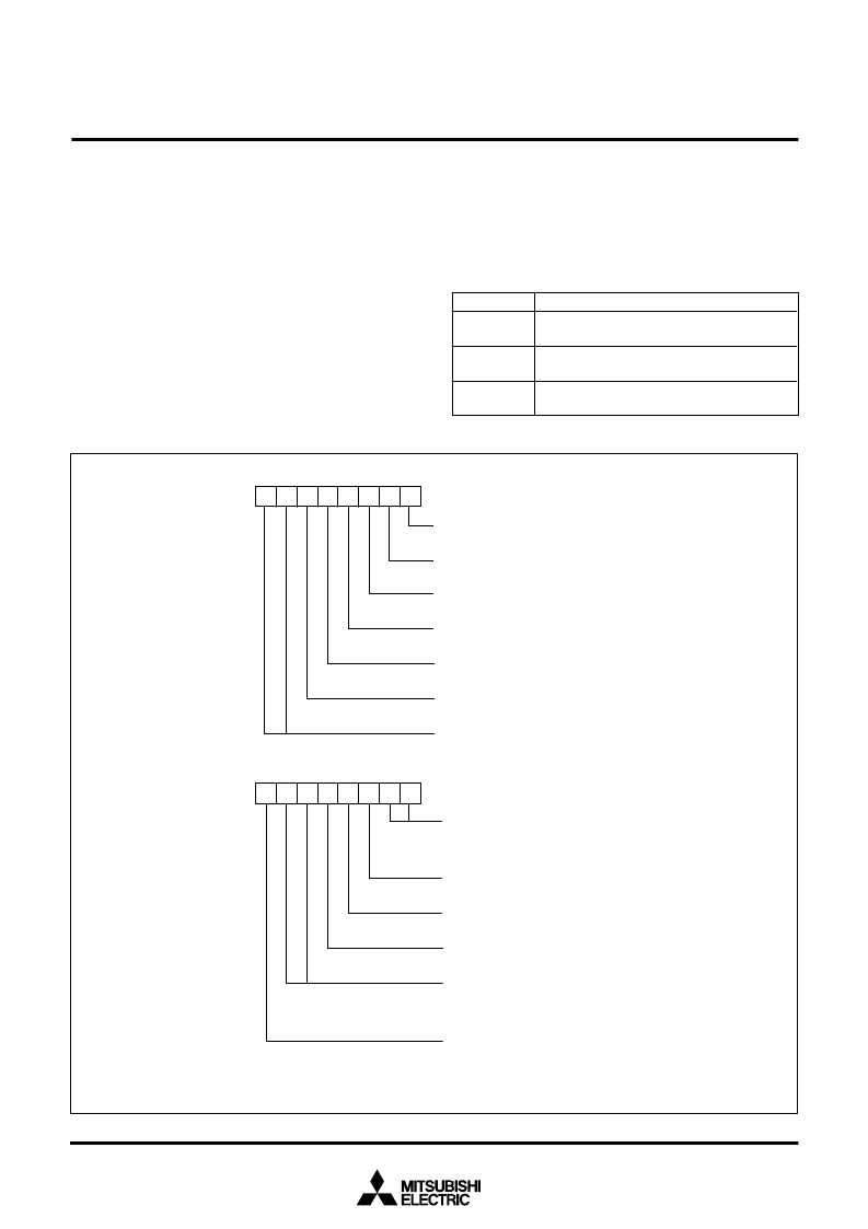
Fig. 28 Structure of segment output enable register and LCD mode register
enable bit is set to “1” after data is set in the LCD mode register,
the segment output enable register and the LCD display RAM, the
LCD drive control circuit starts reading the display data automati-
cally, performs the bias control and the duty ratio control, and dis-
plays the data on the LCD panel.
Table 8. Maximum number of display pixels at each duty ratio
Duty ratio
Maximum number of display pixel
80 dots
or 8 segment LCD 10 digits
120 dots
or 8 segment LCD 15 digits
160 dots
or 8 segment LCD 20 digits
2
3
4
Segment output enable bit 0
0 : Output ports P3
0
–P3
5
1 : Segment output SEG
18
–SEG
23
Segment output enable bit 1
0 : Output ports P3
6
, P3
7
1 : Segment output SEG
24
,SEG
25
Segment output enable bit 2
0 : Output ports P0
0
–P0
5
1 : Segment output SEG
26
–SEG
31
Segment output enable bit 3
0 : Output ports P0
6
,P0
7
1 : Segment output SEG
32
,SEG
33
Segment output enable bit 4
0 : Output port P1
0
1 : Segment output SEG
34
Segment output enable bit 5
0 : Output ports P1
1
–P1
5
1 : Segment output SEG
35
–SEG
39
Not used (return “0” when read)
(Do not write “1” to this bit)
Segment output enable register
(SEG : address 0038
16
)
b7
b0
LCD mode register
(LM : address 0039
16
)
Duty ratio selection bits
0 0 : Not used
0 1 : 2 duty (use COM
0
, COM
1
)
1 0 : 3 duty (use COM
0
–COM
2
)
1 1 : 4 duty (use COM
0
–COM
3
)
Bias control bit
0 : 1/3 bias
1 : 1/2 bias
LCD enable bit
0 : LCD OFF
1 : LCD ON
Voltage multiplier control bit
0 : Voltage multiplier disable
1 : Voltage multiplier enable
LCD circuit divider division ratio selection bits
0 0 : Clock input
0 1 : 2 division of Clock input
1 0 : 4 division of Clock input
1 1 : 8 division of Clock input
LCDCK count source selection bit (Note)
0 : f(X
CIN
)/32
1 : f(X
IN
)/8192 (f(X
CIN
)/8192 in low-speed mode)
Note :
LCDCK is a clock for a LCD timing controller.
b7
b0
相關(guān)PDF資料 |
PDF描述 |
|---|---|
| M38257M8-062FP | SINGLE-CHIP 8-BIT CMOS MICROCOMPUTER |
| M38257M8-080FP | SINGLE-CHIP 8-BIT CMOS MICROCOMPUTER |
| M38257M8-140GP | SINGLE-CHIP 8-BIT CMOS MICROCOMPUTER |
| M38257M8D090FP | SINGLE-CHIP 8-BIT CMOS MICROCOMPUTER |
| M38272E5MXXXFP | Single, Low Power, Rail-to-Rail Input/Output Operational Amplifier 8-SOIC 0 to 70 |
相關(guān)代理商/技術(shù)參數(shù) |
參數(shù)描述 |
|---|---|
| M38258MCM084 | 制造商:Panasonic Industrial Company 功能描述:IC |
| M3826 | 功能描述:電纜固定件和配件 LTRSCG 1000 BLACK RoHS:否 制造商:Heyco 類型:Cable Grips, Liquid Tight 材料:Nylon 顏色:Black 安裝方法:Cable 最大光束直徑:11.4 mm 抗拉強(qiáng)度: |
| M3826 BK001 | 制造商:Alpha Wire Company 功能描述:CBL 2COND 16AWG BLK 1000' |
| M3826 BK002 | 制造商:Alpha Wire Company 功能描述:CBL 2COND 16AWG BLK 500' |
| M3826 BK005 | 制造商:Alpha Wire Company 功能描述:CBL 2COND 16AWG BLK 100' |
發(fā)布緊急采購,3分鐘左右您將得到回復(fù)。