- 您現(xiàn)在的位置:買賣IC網(wǎng) > PDF目錄370892 > M38192E8-XXXFP (Mitsubishi Electric Corporation) SINGLE-CHIP 8-BIT CMOS MICROCOMPUTER PDF資料下載
參數(shù)資料
| 型號: | M38192E8-XXXFP |
| 廠商: | Mitsubishi Electric Corporation |
| 英文描述: | SINGLE-CHIP 8-BIT CMOS MICROCOMPUTER |
| 中文描述: | 單芯片8位CMOS微機(jī) |
| 文件頁數(shù): | 11/60頁 |
| 文件大小: | 664K |
| 代理商: | M38192E8-XXXFP |
第1頁第2頁第3頁第4頁第5頁第6頁第7頁第8頁第9頁第10頁當(dāng)前第11頁第12頁第13頁第14頁第15頁第16頁第17頁第18頁第19頁第20頁第21頁第22頁第23頁第24頁第25頁第26頁第27頁第28頁第29頁第30頁第31頁第32頁第33頁第34頁第35頁第36頁第37頁第38頁第39頁第40頁第41頁第42頁第43頁第44頁第45頁第46頁第47頁第48頁第49頁第50頁第51頁第52頁第53頁第54頁第55頁第56頁第57頁第58頁第59頁第60頁
11
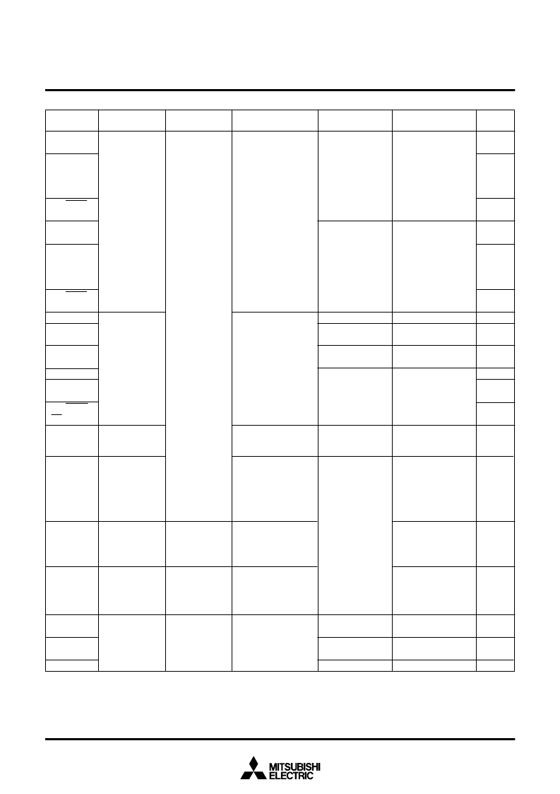
3819 Group
SINGLE-CHIP 8-BIT CMOS MICROCOMPUTER
MITSUBISHI MICROCOMPUTERS
P6
2
/CNTR
0
,
P6
3
/CNTR
1
P6
4
/S
IN1
P6
5
/S
OUT1
,
P6
6
/S
CLK11
P6
7
/S
RDY1
/
CS/S
CLK12
Port P5
Pin
Name
Input/Output
I/O Format
Non-Port Function
Related SFR
S
Diagram
No.
P5
0
/S
IN2
/
AN
8
P5
1
/S
OUT2
/
AN
9
,
P5
2
/S
CLK2
/
AN
10
P5
3
/S
RDY2
/
AN
11
P5
4
/S
IN3
/
AN
12
P5
5
/S
OUT3
/
AN
13
,
P5
6
/S
CLK3
/
AN
14
P5
7
/S
RDY3
/
AN
15
P6
0
CMOS compatible
input level
CMOS 3-state output
Input/output,
individual bits
Serial I/O2 func-
tion I/O
A-D conversion in-
put
Serial I/O2 control
register
AD/DA control regis-
ter
(9)
Serial I/O3 func-
tion I/O
A-D conversion in-
put
Serial I/O3 control
register
AD/DA control regis-
ter
Timer 56 mode regis-
ter
PWM (timer) out-
put
P6
1
/PWM
Timer input
Interrupt edge selec-
tion register
Serial I/O1 func-
tion I/O
Serial I/O1 control
register
Serial I/O automatic
transfer control regis-
ter
CMOS compatible
input level
CMOS 3-state output
CMOS compatible
input level
High-breakdown-
voltage P-channel
open-drain output
with pull-down
resistor
High-breakdown-
voltage P-channel
open-drain output
with pull-down
resistor
CMOS compatible
input level
High-breakdown-
voltage P-channel
open-drain output
P7
0
/AN
0
–
P7
7
/AN
7
P8
0
/SEG
8
–
P8
7
/SEG
15
P9
0
/SEG
16
–
P9
7
/SEG
23
PA
0
/SEG
0
–
PA
7
/SEG
7
PB
0
/X
COUT
,
PB
1
/X
CIN
PB
2
/DA
PB
3
CMOS compatible
input level
CMOS 3-state output
FLD automatic
display function
A-D conversion in-
put
I/O for sub-clock
generating circuit
D-A conversion
output
AD/DA control regis-
ter
FLDC mode register
Segment/port switch
register
FLDC mode register
FLDC mode register
Segment/port switch
register
CPU mode register
AD/DA control regis-
ter
Output
Input/output,
individual bits
Input/output,
individual bits
Port P6
Port P7
Port P8
Port P9
Port PA
(10)
(11)
(9)
(10)
(11)
(4)
(8)
(7)
(9)
(10)
(11)
(12)
(13)
(5)
(13)
(14)
(15)
(16)
Note :
Make sure that the input level at each pin is either 0 V or V
CC
during execution of the STP instruction. When an input level is at an intermediate poten-
tial, a current will flow from V
CC
to V
SS
through the input-stage gate.
Port PB
CMOS compatible
input level
CMOS 3-state output
(4)
相關(guān)PDF資料 |
PDF描述 |
|---|---|
| M38192E8-XXXFS | SINGLE-CHIP 8-BIT CMOS MICROCOMPUTER |
| M38192EC-XXXFP | SINGLE-CHIP 8-BIT CMOS MICROCOMPUTER |
| M38192EC-XXXFS | SINGLE-CHIP 8-BIT CMOS MICROCOMPUTER |
| M38192ED-XXXFP | SINGLE-CHIP 8-BIT CMOS MICROCOMPUTER |
| M38192ED-XXXFS | SINGLE-CHIP 8-BIT CMOS MICROCOMPUTER |
相關(guān)代理商/技術(shù)參數(shù) |
參數(shù)描述 |
|---|---|
| M38197MA127F | 制造商:Panasonic Industrial Company 功能描述:IC |
| M38197MA131F | 制造商:Panasonic Industrial Company 功能描述:IC |
| M38197MA137F | 制造商:Panasonic Industrial Company 功能描述:IC |
| M38197MA161F | 制造商:Panasonic Industrial Company 功能描述:IC |
| M38197MA181F | 制造商:Panasonic Industrial Company 功能描述:IC |
發(fā)布緊急采購,3分鐘左右您將得到回復(fù)。