- 您現(xiàn)在的位置:買(mǎi)賣(mài)IC網(wǎng) > PDF目錄45034 > M37540M4V-XXXFP 8-BIT, MROM, 6 MHz, MICROCONTROLLER, PQFP32 PDF資料下載
參數(shù)資料
| 型號(hào): | M37540M4V-XXXFP |
| 元件分類(lèi): | 微控制器/微處理器 |
| 英文描述: | 8-BIT, MROM, 6 MHz, MICROCONTROLLER, PQFP32 |
| 封裝: | 7 X 7 MM, 0.80 MM PITCH, PLASTIC, LQFP-32 |
| 文件頁(yè)數(shù): | 35/88頁(yè) |
| 文件大?。?/td> | 872K |
| 代理商: | M37540M4V-XXXFP |
第1頁(yè)第2頁(yè)第3頁(yè)第4頁(yè)第5頁(yè)第6頁(yè)第7頁(yè)第8頁(yè)第9頁(yè)第10頁(yè)第11頁(yè)第12頁(yè)第13頁(yè)第14頁(yè)第15頁(yè)第16頁(yè)第17頁(yè)第18頁(yè)第19頁(yè)第20頁(yè)第21頁(yè)第22頁(yè)第23頁(yè)第24頁(yè)第25頁(yè)第26頁(yè)第27頁(yè)第28頁(yè)第29頁(yè)第30頁(yè)第31頁(yè)第32頁(yè)第33頁(yè)第34頁(yè)當(dāng)前第35頁(yè)第36頁(yè)第37頁(yè)第38頁(yè)第39頁(yè)第40頁(yè)第41頁(yè)第42頁(yè)第43頁(yè)第44頁(yè)第45頁(yè)第46頁(yè)第47頁(yè)第48頁(yè)第49頁(yè)第50頁(yè)第51頁(yè)第52頁(yè)第53頁(yè)第54頁(yè)第55頁(yè)第56頁(yè)第57頁(yè)第58頁(yè)第59頁(yè)第60頁(yè)第61頁(yè)第62頁(yè)第63頁(yè)第64頁(yè)第65頁(yè)第66頁(yè)第67頁(yè)第68頁(yè)第69頁(yè)第70頁(yè)第71頁(yè)第72頁(yè)第73頁(yè)第74頁(yè)第75頁(yè)第76頁(yè)第77頁(yè)第78頁(yè)第79頁(yè)第80頁(yè)第81頁(yè)第82頁(yè)第83頁(yè)第84頁(yè)第85頁(yè)第86頁(yè)第87頁(yè)第88頁(yè)
7540 Group
Rev.4.00
Jun 21, 2004
page 40 of 82
REJ03B0011-0400Z
A/D Converter
The functional blocks of the A/D converter are described below.
[A/D conversion register] AD
The A/D conversion register is a read-only register that stores the
result of A/D conversion. Do not read out this register during an A/
D conversion.
[A/D control register] ADCON
The A/D control register controls the A/D converter. Bit 2 to 0 are
analog input pin selection bits. Bit 4 is the AD conversion comple-
tion bit. The value of this bit remains at “0” during A/D conversion,
and changes to “1” at completion of A/D conversion.
A/D conversion is started by setting this bit to “0”.
[Comparison voltage generator]
The comparison voltage generator divides the voltage between
AVSS and VREF by 1024, and outputs the divided voltages.
[Channel selector]
The channel selector selects one of ports P27/AN7 to P20/AN0,
and inputs the voltage to the comparator.
[Comparator and control circuit]
The comparator and control circuit compares an analog input volt-
age with the comparison voltage and stores its result into the A/D
conversion register. When A/D conversion is completed, the con-
trol circuit sets the AD conversion completion bit and the AD
interrupt request bit to “1”. Because the comparator is constructed
linked to a capacitor, set f(XIN) to 500 kHz or more during A/D con-
version.
s Note on A/D converter
As for AD translation accuracy, on the following operating condi-
tions, accuracy may become low.
(1) Since the analog circuit inside a microcomputer becomes sensi-
tive to noise when VREF voltage is set up lower than Vcc
voltage, accuracy may become low rather than the case where
VREF voltage and Vcc voltage are set up to the same value.
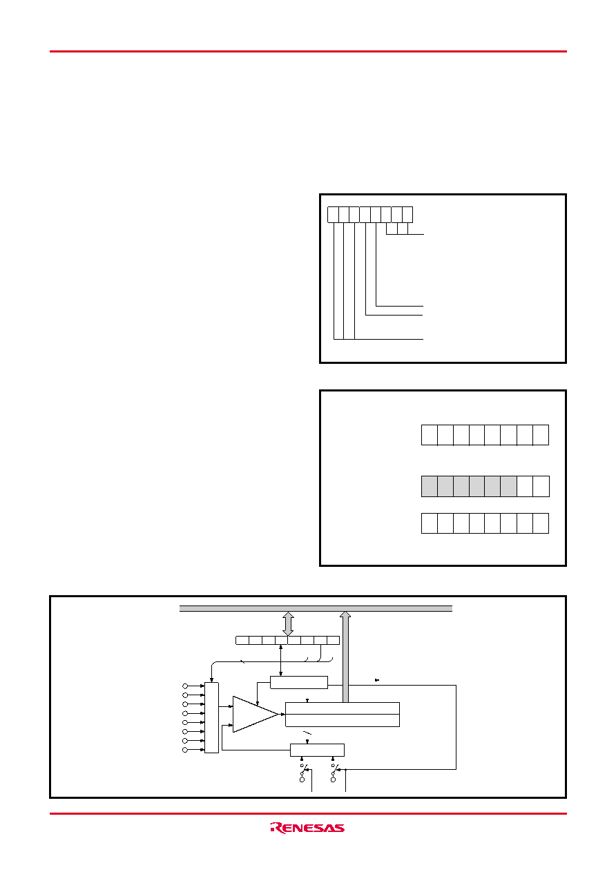
Fig. 38 Structure of A/D control register
Fig. 39 Structure of A/D conversion register
Fig. 40 Block diagram of A/D converter
A/D control register
(ADCON : address 003416, initial value: 1016)
Not used (returns “0” when read)
AD conversion completion bit
0 : Conversion in progress
1 : Conversion completed
b7
b0
Analog input pin selection bits
000 : P20/AN0
001 : P21/AN1
010 : P22/AN2
011 : P23/AN3
100 : P24/AN4
101 : P25/AN5
110 : P26/AN6 (Note)
111 : P27/AN7 (Note)
Note: These can be used only for 36 pin version.
Read 8-bit (Read only address 003516)
b7
b0
b9
b8
b7
b6
b5
b4
b3
b2
(Address 003516)
Read 10-bit (read in order address 003616, 003516)
b7
b0
b9
b8
(Address 003616)
b7
b0
b7
b6
b5
b4
b3
b2
b1
b0
(Address 003516)
Note: High-order 6-bit of address 003616 returns “0” when read.
A/D control register
(Address 003416)
Channel
selector
A/D control circuit
Resistor ladder
VREF
Comparator
A/D interrupt request
b7
b0
Data bus
3
10
P20/AN0
P21/AN1
P22/AN2
P23/AN3
P24/AN4
P25/AN5
P26/AN6
P27/AN7
A/D conversion register (low-order)
(Address 003616)
(Address 003516)
A/D conversion register (high-order)
VSS
(2) When VREF voltage is lower than [3.0 V], the accuracy at the
low temperature may become extremely low compared with
that at room temperature When the system would be used at
low temperature, the use at VREF=3.0 V or more is recom-
mended.
相關(guān)PDF資料 |
PDF描述 |
|---|---|
| M37540M2T-XXXGP | 8-BIT, MROM, 6 MHz, MICROCONTROLLER, PDSO36 |
| M37540E8GP | 8-BIT, OTPROM, 6 MHz, MICROCONTROLLER, PDSO36 |
| M37540M4-XXXSP | 8-BIT, MROM, 6 MHz, MICROCONTROLLER, PDIP32 |
| M37540E8T-XXXFP | 8-BIT, OTPROM, 6 MHz, MICROCONTROLLER, PQFP32 |
| M37540E2FP | 8-BIT, OTPROM, 6 MHz, MICROCONTROLLER, PQFP32 |
相關(guān)代理商/技術(shù)參數(shù) |
參數(shù)描述 |
|---|---|
| M37540M4V-XXXGP | 制造商:RENESAS 制造商全稱(chēng):Renesas Technology Corp 功能描述:8-BIT CISC SINGLE-CHIP MICROCOMPUTER 740 FAMILY / 740 SERIES |
| M37540M4-XXXFP | 制造商:RENESAS 制造商全稱(chēng):Renesas Technology Corp 功能描述:8-BIT CISC SINGLE-CHIP MICROCOMPUTER 740 FAMILY / 740 SERIES |
| M37540M4-XXXGP | 制造商:RENESAS 制造商全稱(chēng):Renesas Technology Corp 功能描述:SINGLE-CHIP 8-BIT CMOS MICROCOMPUTER |
| M37540M4-XXXSP | 制造商:RENESAS 制造商全稱(chēng):Renesas Technology Corp 功能描述:8-BIT CISC SINGLE-CHIP MICROCOMPUTER 740 FAMILY / 740 SERIES |
| M37540MXT-XXXGP | 制造商:RENESAS 制造商全稱(chēng):Renesas Technology Corp 功能描述:SINGLE-CHIP 8-BIT CMOS MICROCOMPUTER |
發(fā)布緊急采購(gòu),3分鐘左右您將得到回復(fù)。