- 您現在的位置:買賣IC網 > PDF目錄45034 > M37540M2-XXXGP 8-BIT, MROM, 6 MHz, MICROCONTROLLER, PDSO36 PDF資料下載
參數資料
| 型號: | M37540M2-XXXGP |
| 元件分類: | 微控制器/微處理器 |
| 英文描述: | 8-BIT, MROM, 6 MHz, MICROCONTROLLER, PDSO36 |
| 封裝: | 0.450 INCH, 0.80 MM PITCH, PLASTIC, SSOP-36 |
| 文件頁數: | 67/88頁 |
| 文件大?。?/td> | 872K |
| 代理商: | M37540M2-XXXGP |
第1頁第2頁第3頁第4頁第5頁第6頁第7頁第8頁第9頁第10頁第11頁第12頁第13頁第14頁第15頁第16頁第17頁第18頁第19頁第20頁第21頁第22頁第23頁第24頁第25頁第26頁第27頁第28頁第29頁第30頁第31頁第32頁第33頁第34頁第35頁第36頁第37頁第38頁第39頁第40頁第41頁第42頁第43頁第44頁第45頁第46頁第47頁第48頁第49頁第50頁第51頁第52頁第53頁第54頁第55頁第56頁第57頁第58頁第59頁第60頁第61頁第62頁第63頁第64頁第65頁第66頁當前第67頁第68頁第69頁第70頁第71頁第72頁第73頁第74頁第75頁第76頁第77頁第78頁第79頁第80頁第81頁第82頁第83頁第84頁第85頁第86頁第87頁第88頁
7540 Group
Rev.4.00
Jun 21, 2004
page 7 of 82
REJ03B0011-0400Z
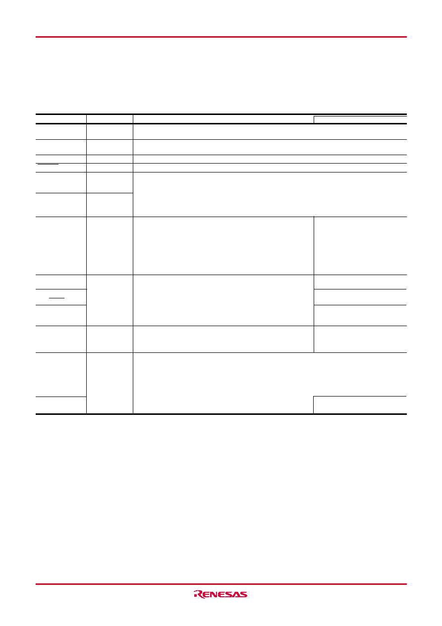
PIN DESCRIPTION
Table 1 Pin description
Function
Apply voltage of 2.2 to 5.5 V to Vcc, and 0 V to Vss.
Reference voltage input pin for A/D converter
Chip operating mode control pin, which is always connected to Vss.
Reset input pin for active “L”
Input and output pins for main clock generating circuit
Connect a ceramic resonator or quartz crystal oscillator between the XIN and XOUT pins.
For using RC oscillator, short between the XIN and XOUT pins, and connect the capacitor and resistor.
If an external clock is used, connect the clock source to the XIN pin and leave the XOUT pin open.
When the on-chip oscillator is selected as the main clock, connect XIN pin to VSS and leave XOUT open.
Function expect a port function
Name
Power source
(Note 1)
Analog reference
voltage
CNVss
Reset input
Clock input
I/O port P0
I/O port P1
Pin
Vcc, Vss
VREF
CNVss
RESET
XIN
P00/CNTR1
P01/TYOUT
P02/TZOUT
P03/TXOUT
P04–P07
Notes 1: VCC = 2.4 to 5.5 V for the extended operating temperature version and the extended operating temperature 125 °C version.
2: P26/AN6 and P27/AN7 do not exist for the 32-pin version, so that Port P2 is a 6-bit I/O port.
3: P35 and P36/INT1 do not exist for the 32-pin version, so that Port P3 is a 6-bit I/O port.
Key-input (key-on wake up
interrupt input) pins
Timer Y, timer Z, timer X and
timer A function pin
8-bit I/O port.
I/O direction register allows each pin to be individually pro-
grammed as either input or output.
CMOS compatible input level
CMOS 3-state output structure
Whether a built-in pull-up resistor is to be used or not can be de-
termined by program.
5-bit I/O port
I/O direction register allows each pin to be individually pro-
grammed as either input or output.
CMOS compatible input level
CMOS 3-state output structure
CMOS/TTL level can be switched for P10, P12 and P13
8-bit I/O port having almost the same function as P0
CMOS compatible input level
CMOS 3-state output structure
8-bit I/O port
P10/RxD1
P11/TxD1
P12/SCLK1/SCLK2
P13/SRDY1/SDATA2
P14/CNTR0
P20/AN0–P27/AN7
P30–P35
P36/INT1
P37/INT0
I/O port P2
(Note 2)
I/O port P3
(Note 3)
Serial I/O1 function pin
Serial I/O2 function pin
Timer X function pin
Input pins for A/D converter
Interrupt input pins
I/O direction register allows each pin to be individually programmed as either input or output.
CMOS compatible input level (CMOS/TTL level can be switched for P36 and P37).
CMOS 3-state output structure
P30 to P36 can output a large current for driving LED.
XOUT
Clock output
Whether a built-in pull-up resistor is to be used or not can be de-
termined by program.
相關PDF資料 |
PDF描述 |
|---|---|
| M37540M4V-XXXFP | 8-BIT, MROM, 6 MHz, MICROCONTROLLER, PQFP32 |
| M37540M2T-XXXGP | 8-BIT, MROM, 6 MHz, MICROCONTROLLER, PDSO36 |
| M37540E8GP | 8-BIT, OTPROM, 6 MHz, MICROCONTROLLER, PDSO36 |
| M37540M4-XXXSP | 8-BIT, MROM, 6 MHz, MICROCONTROLLER, PDIP32 |
| M37540E8T-XXXFP | 8-BIT, OTPROM, 6 MHz, MICROCONTROLLER, PQFP32 |
相關代理商/技術參數 |
參數描述 |
|---|---|
| M37540M2-XXXSP | 制造商:RENESAS 制造商全稱:Renesas Technology Corp 功能描述:SINGLE-CHIP 8-BIT CMOS MICROCOMPUTER |
| M37540M4 | 制造商:MITSUBISHI 制造商全稱:Mitsubishi Electric Semiconductor 功能描述:SINGLE-CHIP 8-BIT CMOS MICROCOMPUTER |
| M37540M4T-XXXFP | 制造商:RENESAS 制造商全稱:Renesas Technology Corp 功能描述:8-BIT CISC SINGLE-CHIP MICROCOMPUTER 740 FAMILY / 740 SERIES |
| M37540M4T-XXXGP | 制造商:RENESAS 制造商全稱:Renesas Technology Corp 功能描述:SINGLE-CHIP 8-BIT CMOS MICROCOMPUTER |
| M37540M4V-XXXFP | 制造商:RENESAS 制造商全稱:Renesas Technology Corp 功能描述:8-BIT CISC SINGLE-CHIP MICROCOMPUTER 740 FAMILY / 740 SERIES |
發(fā)布緊急采購,3分鐘左右您將得到回復。