- 您現(xiàn)在的位置:買賣IC網(wǎng) > PDF目錄98006 > M37534M4-XXXGP 8-BIT, MROM, 6 MHz, MICROCONTROLLER, PQFP32 PDF資料下載
參數(shù)資料
| 型號: | M37534M4-XXXGP |
| 元件分類: | 微控制器/微處理器 |
| 英文描述: | 8-BIT, MROM, 6 MHz, MICROCONTROLLER, PQFP32 |
| 封裝: | 7 X 7 MM, 0.80 MM PITCH, PLASTIC, LQFP-32 |
| 文件頁數(shù): | 36/58頁 |
| 文件大?。?/td> | 753K |
| 代理商: | M37534M4-XXXGP |
第1頁第2頁第3頁第4頁第5頁第6頁第7頁第8頁第9頁第10頁第11頁第12頁第13頁第14頁第15頁第16頁第17頁第18頁第19頁第20頁第21頁第22頁第23頁第24頁第25頁第26頁第27頁第28頁第29頁第30頁第31頁第32頁第33頁第34頁第35頁當(dāng)前第36頁第37頁第38頁第39頁第40頁第41頁第42頁第43頁第44頁第45頁第46頁第47頁第48頁第49頁第50頁第51頁第52頁第53頁第54頁第55頁第56頁第57頁第58頁
7534 Group
Rev.3.00
Oct 23, 2006
page 39 of 53
REJ03B0099-0300
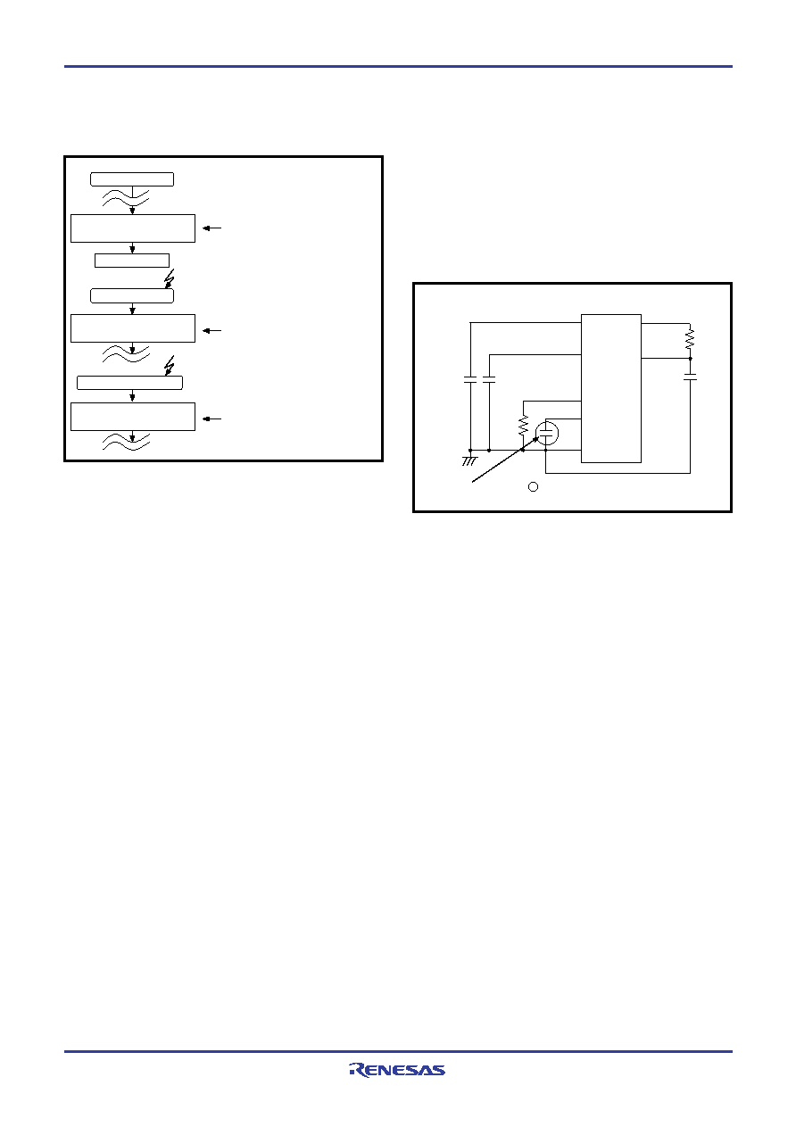
Note on A/D Converter
Method to stabilize A/D Converter is described below.
(a) A/D conversion accuracy could be affected for Bus Powered*1
USB devices, while the communicating.
Figure 48 shows the method to stabilize A/D conversion accu-
racy, inserting a capacitor between Vref and VSS.
*1: Power supplied by USB VCC BUS.
(b) It is recommended for A/D accuracy to avoid converting while
USB communication, and use average value of several con-
verted values.
DATA REQUIRED FOR MASK ORDERS
The following are necessary when ordering a mask ROM produc-
tion:
(1) Mask ROM Order Confirmation Form
(2) Mark Specification Form
(3) Data to be written to ROM, in EPROM form
................................... (three identical copies) or one floppy disk
* For the mask ROM confirmation and the mark specifications,
refer to the “Renesas Technology Corp.” Homepage
(http://www.renesas.com).
One Time PROM Version
The CNVss pin is connected to the internal memory circuit block by a
low-ohmic resistance, since it has the multiplexed function to be a
programmable power source pin (VPP pin) as well.
To improve the noise reduction, connect a track between CNVss pin
and Vss pin with 1 to 10 k
resistance.
The mask ROM version track of CNVss pin has no operational inter-
ference even if it is connected via a resistor.
Electric Characteristic Differences Among
Mask ROM and One TIme PROM Version MCUs
There are differences in electric characteristics, operation margin,
noise immunity, and noise radiation among mask ROM and One
Time PROM version MCUs due to the differences in the manufac-
turing processes.
When manufacturing an application system with One Time PROM
version and then switching to use of the mask ROM version, per-
form sufficient evaluations for the commercial samples of the
mask ROM version.
Note on Power Source Voltage
When the power source voltage value of a microcomputer is less
than the value which is indicated as the recommended operating
conditions, the microcomputer does not operate normally and may
perform unstable operation.
In a system where the power source voltage drops slowly when
the power source voltage drops or the power supply is turned off,
reset a microcomputer when the supply voltage is less than the
recommended operating conditions and design a system not to
cause errors to the system by this unstable operation.
SUSPEND Routine
RESUME Routine
STP
Configuration to CMOS input
level for P10, P12, P13 input level.
Remote wake up Routine
P1P3C xxxxx0xx2
Configuration to CMOS
input level for P10, P12, P13
input level.
P1P3C xxxxx1xx2
Configuration to TTL input
level for P10, P12, P13 input
level.
P1P3C xxxxx1xx2
Configuration to TTL input
level for P10, P12, P13 input
level.
Configuration to TTL input level
for P10, P12, P13 input level.
Configuration to TTL input level
for P10, P12, P13 input level.
Fig. 47 Countermeasure (2) by software
Fig. 48 Method to stabilize A/D conversion accuracy
AN0 to AN7
Vcc
CNVss
1
F
0.01 to 1
F
Vref
Vss
1 to 10 k
0.1 to 1
F
: Recommends for A/D accuracy
0.22
F
7534 Group
1.5 k
USBVREFOUT
D-
相關(guān)PDF資料 |
PDF描述 |
|---|---|
| M37534M4-XXXGP | 8-BIT, MROM, 6 MHz, MICROCONTROLLER, PQFP32 |
| M37534E4GP | 8-BIT, OTPROM, 6 MHz, MICROCONTROLLER, PQFP32 |
| M37548G3FP | 8-BIT, MROM, 8 MHz, MICROCONTROLLER, PDSO20 |
| M37548G1FP | 8-BIT, MROM, 8 MHz, MICROCONTROLLER, PDSO20 |
| M37548G2-XXXFP | 8-BIT, MROM, 8 MHz, MICROCONTROLLER, PDSO20 |
相關(guān)代理商/技術(shù)參數(shù) |
參數(shù)描述 |
|---|---|
| M37534M4-XXXSP | 制造商:RENESAS 制造商全稱:Renesas Technology Corp 功能描述:SINGLE-CHIP 8-BIT CMOS MICROCOMPUTER |
| M37534RSS | 制造商:RENESAS 制造商全稱:Renesas Technology Corp 功能描述:SINGLE-CHIP 8-BIT CMOS MICROCOMPUTER |
| M37536E8SP | 制造商:MITSUBISHI 制造商全稱:Mitsubishi Electric Semiconductor 功能描述:SINGLE-CHIP 8-BIT CMOS MICROCOMPUTER |
| M37536M4 | 制造商:MITSUBISHI 制造商全稱:Mitsubishi Electric Semiconductor 功能描述:SINGLE-CHIP 8-BIT CMOS MICROCOMPUTER |
| M37536M4-XXXSP | 制造商:MITSUBISHI 制造商全稱:Mitsubishi Electric Semiconductor 功能描述:SINGLE-CHIP 8-BIT CMOS MICROCOMPUTER |
發(fā)布緊急采購,3分鐘左右您將得到回復(fù)。