- 您現(xiàn)在的位置:買賣IC網(wǎng) > PDF目錄45030 > M37272EFFP 8-BIT, OTPROM, 8 MHz, MICROCONTROLLER, PDSO42 PDF資料下載
參數(shù)資料
| 型號: | M37272EFFP |
| 元件分類: | 微控制器/微處理器 |
| 英文描述: | 8-BIT, OTPROM, 8 MHz, MICROCONTROLLER, PDSO42 |
| 封裝: | 0.450 INCH, 0.80 MM PITCH, PLASTIC, SSOP-42 |
| 文件頁數(shù): | 101/131頁 |
| 文件大小: | 1297K |
| 代理商: | M37272EFFP |
第1頁第2頁第3頁第4頁第5頁第6頁第7頁第8頁第9頁第10頁第11頁第12頁第13頁第14頁第15頁第16頁第17頁第18頁第19頁第20頁第21頁第22頁第23頁第24頁第25頁第26頁第27頁第28頁第29頁第30頁第31頁第32頁第33頁第34頁第35頁第36頁第37頁第38頁第39頁第40頁第41頁第42頁第43頁第44頁第45頁第46頁第47頁第48頁第49頁第50頁第51頁第52頁第53頁第54頁第55頁第56頁第57頁第58頁第59頁第60頁第61頁第62頁第63頁第64頁第65頁第66頁第67頁第68頁第69頁第70頁第71頁第72頁第73頁第74頁第75頁第76頁第77頁第78頁第79頁第80頁第81頁第82頁第83頁第84頁第85頁第86頁第87頁第88頁第89頁第90頁第91頁第92頁第93頁第94頁第95頁第96頁第97頁第98頁第99頁第100頁當前第101頁第102頁第103頁第104頁第105頁第106頁第107頁第108頁第109頁第110頁第111頁第112頁第113頁第114頁第115頁第116頁第117頁第118頁第119頁第120頁第121頁第122頁第123頁第124頁第125頁第126頁第127頁第128頁第129頁第130頁第131頁
71
SINGLE-CHIP 8-BIT CMOS MICROCOMPUTER with CLOSED CAPTION DECODER
and ON-SCREEN DISPLAY CONTROLLER
M37272M6H/M8H/MAH/MFH–XXXSP/FP
M37272E8SP/FP, M37272EFSP/FP
MITSUBISHI MICROCOMPUTERS
Rev. 1.0
8.11.4 Field Determination Display
To display the block with vertical dot size of 1/2H, whether an even
field or an odd field is determined through differences in a synchro-
nizing signal waveform of interlacing system. The dot line 0 or 1 (re-
fer to Figure 8.11.14) corresponding to the field is displayed alter-
nately.
In the following, the field determination standard for the case where
both the horizontal sync signal and the vertical sync signal are nega-
tive-polarity inputs will be explained. A field determination is deter-
mined by detecting the time from a falling edge of the horizontal sync
signal until a falling edge of the VSYNC control signal (refer to Figure
8.11.6) in the microcomputer and then comparing this time with the
time of the previous field. When the time is longer than the compar-
ing time, it is regarded as even field. When the time is shorter, it is
regarded as odd field
The contents of this field can be read out by the field determination
flag (bit 6 of the I/O polarity control register at address 00D816). A dot
line is specified by bit 5 of the I/O polarity control register (refer to
Figure 8.11.14).
However, the field determination flag read out from the CPU is fixed
to “0” at even field or “1” at odd field, regardless of bit 5.
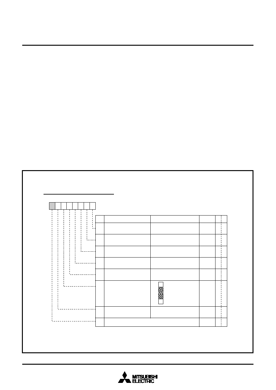
Fig. 8.11.13 I/O Polarity Control Register
0 : “
” at even field
“
” at odd field
1 : “
” at even field
“
” at odd field
b7 b6 b5 b4 b3 b2 b1 b0
I/O polarity control register (PC) [Address 00D8 16]
B
Name
Functions
After reset R W
I/O Polarity Control Register
0HSYNC input polarity
switch bit (PC0)
0 : Positive polarity input
1 : Negative polarity input
0
1
0 : Positive polarity input
1 : Negative polarity input
0
2
R, G, B output polarity
switch bit (PC2)
0 : Positive polarity output
1 : Negative polarity output
0
3
OUT1 output polarity
switch bit (PC3)
0 : Positive polarity output
1 : Negative polarity output
0
4
OUT2 output polarity
switch bit (PC4)
0 : Positive polarity output
1 : Negative polarity output
0
5
Display dot line selection
bit (PC5) (See note)
0
6
Field determination flag
(PC6)
0 : Even field
1 : Odd field
1
7
0
VSYNC input polarity
switch bit (PC1)
RW
R —
RW
Fix this bit to “0.”
Note: Refer to the corresponding figure (8.11.14).
0
相關PDF資料 |
PDF描述 |
|---|---|
| M37272M6H-XXXSP | 8-BIT, MROM, 8.1 MHz, MICROCONTROLLER, PDIP42 |
| M37272M8H-XXXFP | 8-BIT, MROM, 8.1 MHz, MICROCONTROLLER, PDSO42 |
| M37272M8H-XXXSP | 8-BIT, MROM, 8.1 MHz, MICROCONTROLLER, PDIP42 |
| M37272MFH-XXXSP | 8-BIT, MROM, 8.1 MHz, MICROCONTROLLER, PDIP42 |
| M37272MAH-XXXSP | 8-BIT, MROM, 8.1 MHz, MICROCONTROLLER, PDIP42 |
相關代理商/技術(shù)參數(shù) |
參數(shù)描述 |
|---|---|
| M37272EFSP | 制造商:MITSUBISHI 制造商全稱:Mitsubishi Electric Semiconductor 功能描述:SINGLE-CHIP 8-BIT CMOS MICROCOMPUTER with CLOSED CAPTION DECODER and ON-SCREEN DISPLAY CONTROLLER |
| M37272M6 | 制造商:MITSUBISHI 制造商全稱:Mitsubishi Electric Semiconductor 功能描述:SINGLE-CHIP 8-BIT CMOS MICROCOMPUTER with CLOSED CAPTION DECODER and ON-SCREEN DISPLAY CONTROLLER |
| M37272M6-205SP | 制造商:MITSUBISHI 制造商全稱:Mitsubishi Electric Semiconductor 功能描述:SINGLE-CHIP 8-BIT CMOS MICROCOMPUTER with CLOSED CAPTION DECODER and ON-SCREEN DISPLAY CONTROLLER |
| M37272M6327SP | 制造商:MITSUBISHI 功能描述:* |
| M37272M6335SP | 制造商:MITSUBISHI 功能描述:* |
發(fā)布緊急采購,3分鐘左右您將得到回復。