- 您現(xiàn)在的位置:買賣IC網(wǎng) > PDF目錄45027 > M3455AGCFP 4-BIT, OTPROM, 6 MHz, MICROCONTROLLER, PQFP52 PDF資料下載
參數(shù)資料
| 型號: | M3455AGCFP |
| 元件分類: | 微控制器/微處理器 |
| 英文描述: | 4-BIT, OTPROM, 6 MHz, MICROCONTROLLER, PQFP52 |
| 封裝: | 10 X 10 MM, 0.65 MM PITCH, PLASTIC, LQFP-52 |
| 文件頁數(shù): | 89/148頁 |
| 文件大小: | 1807K |
| 代理商: | M3455AGCFP |
第1頁第2頁第3頁第4頁第5頁第6頁第7頁第8頁第9頁第10頁第11頁第12頁第13頁第14頁第15頁第16頁第17頁第18頁第19頁第20頁第21頁第22頁第23頁第24頁第25頁第26頁第27頁第28頁第29頁第30頁第31頁第32頁第33頁第34頁第35頁第36頁第37頁第38頁第39頁第40頁第41頁第42頁第43頁第44頁第45頁第46頁第47頁第48頁第49頁第50頁第51頁第52頁第53頁第54頁第55頁第56頁第57頁第58頁第59頁第60頁第61頁第62頁第63頁第64頁第65頁第66頁第67頁第68頁第69頁第70頁第71頁第72頁第73頁第74頁第75頁第76頁第77頁第78頁第79頁第80頁第81頁第82頁第83頁第84頁第85頁第86頁第87頁第88頁當(dāng)前第89頁第90頁第91頁第92頁第93頁第94頁第95頁第96頁第97頁第98頁第99頁第100頁第101頁第102頁第103頁第104頁第105頁第106頁第107頁第108頁第109頁第110頁第111頁第112頁第113頁第114頁第115頁第116頁第117頁第118頁第119頁第120頁第121頁第122頁第123頁第124頁第125頁第126頁第127頁第128頁第129頁第130頁第131頁第132頁第133頁第134頁第135頁第136頁第137頁第138頁第139頁第140頁第141頁第142頁第143頁第144頁第145頁第146頁第147頁第148頁
Rev.1.02
Nov 26, 2008
Page 45 of 146
REJ03B0224-0102
455A Group
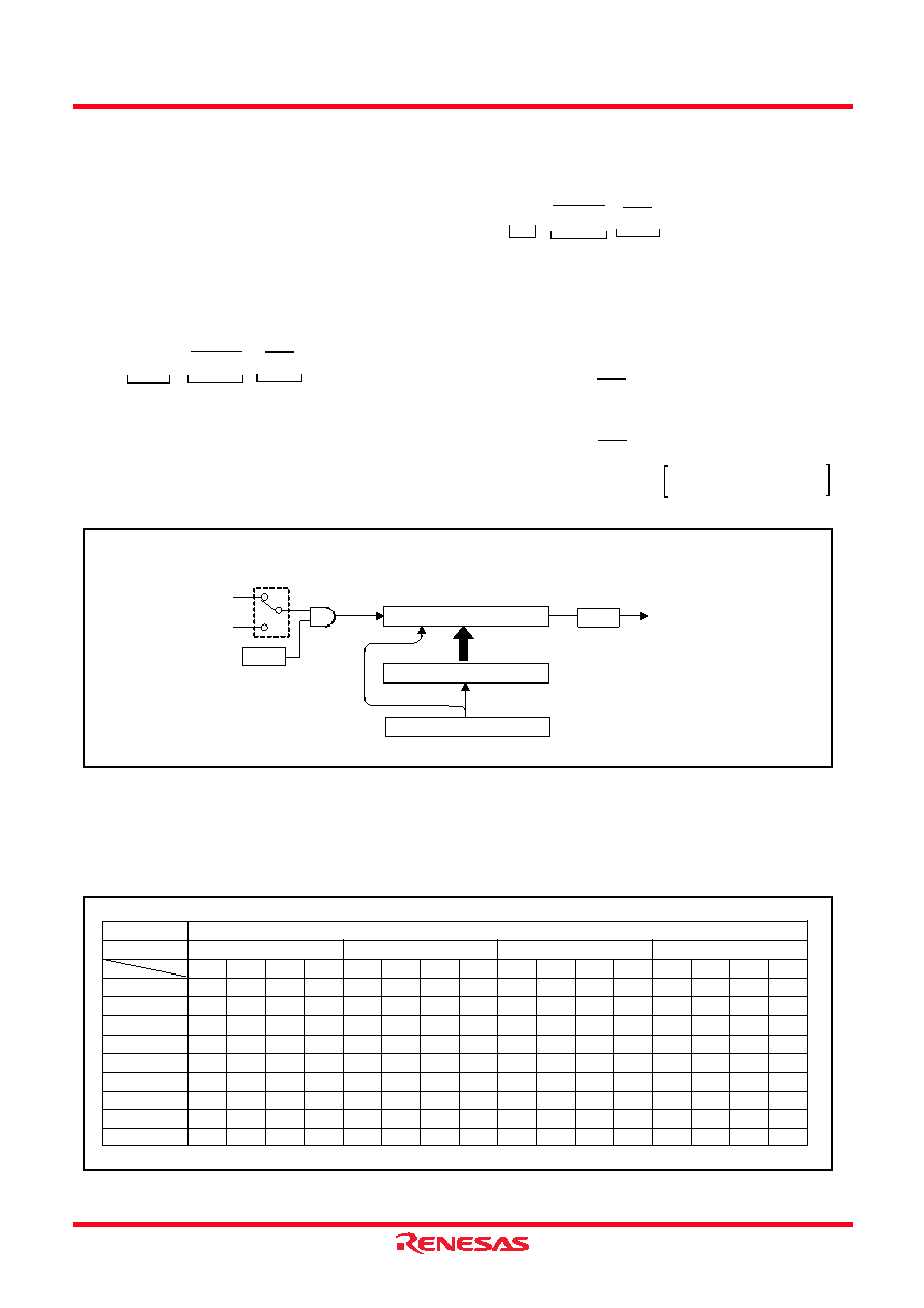
(2) LCD clock control
The LCD clock is determined by the timer LC setting value and
timer LC count source.
After setting data to timer LC, timer LC starts counting by setting
count source with bit 2 of register W4 and setting bit 3 of register
W4 to “1.”
Accordingly, the frequency (F) of the LCD clock is obtained by
the following formula. Numbers ((1) to (3)) shown below the
formula correspond to numbers in Figure 44, respectively.
When using the system clock (STCK) as timer LC count
source (W42=“1”)
When using the bit 4 of timer 3 as timer LC count source
(W42=“0”)
The frame frequency and frame period for each display method
can be obtained by the following formula:
Fig 44. LCD clock control circuit structure
(3) LCD RAM
RAM contains areas corresponding to the liquid crystal display.
When “1” is written to this LCD RAM, the display pixel
corresponding to the bit is automatically displayed.
Fig 45. LCD RAM map
F = STCK
×
(1)
(2)
(3)
[LC: 0 to 15]
LC + 1
1
2
1
F = T34
×
(1)
(2)
(3)
[LC: 0 to 15]
LC + 1
1
2
1
Frame frequency =
(Hz)
Frame frequency =
(Hz)
F: LCD clock frequency
1/n: Duty
n
F
n
Timer LC (4)
Reload register RLC (4)
(TLCA)
Register A
1/2
LCD clock
(TLCA)
W42
0
1
W43
T34
STCK
(3)
(1)
(2)
Z
X
1
8
9
10
11
12
13
14
15
COM
Y
bit
12
SEG0
SEG1
0
SEG2
SEG3
SEG4
SEG5
SEG6
SEG7
COM0
SEG0
SEG1
1
SEG2
SEG3
SEG4
SEG5
SEG6
SEG7
COM1
SEG0
SEG1
2
SEG2
SEG3
SEG4
SEG5
SEG6
SEG7
COM2
SEG0
SEG1
3
SEG2
SEG3
SEG4
SEG5
SEG6
SEG7
COM3
13
SEG8
SEG9
0
SEG10
SEG11
SEG12
SEG13
SEG14
SEG15
COM0
SEG8
SEG9
1
SEG10
SEG11
SEG12
SEG13
SEG14
SEG15
COM1
SEG8
SEG9
2
SEG10
SEG11
SEG12
SEG13
SEG14
SEG15
COM2
SEG8
SEG9
3
SEG10
SEG11
SEG12
SEG13
SEG14
SEG15
COM3
14
SEG16
SEG17
0
SEG18
SEG19
SEG20
SEG21
SEG22
SEG23
COM0
SEG16
SEG17
1
SEG18
SEG19
SEG20
SEG21
SEG22
SEG23
COM1
SEG16
SEG17
2
SEG18
SEG19
SEG20
SEG21
SEG22
SEG23
COM2
SEG16
SEG17
3
SEG18
SEG19
SEG20
SEG21
SEG22
SEG23
COM3
15
SEG24
SEG25
0
SEG26
SEG27
SEG28
SEG29
SEG30
SEG31
COM0
SEG24
SEG25
1
SEG26
SEG27
SEG28
SEG29
SEG30
SEG31
COM1
SEG24
SEG25
2
SEG26
SEG27
SEG28
SEG29
SEG30
SEG31
COM2
SEG24
SEG25
3
SEG26
SEG27
SEG28
SEG29
SEG30
SEG31
COM3
相關(guān)PDF資料 |
PDF描述 |
|---|---|
| M3455AGC-XXXFP | 4-BIT, OTPROM, 6 MHz, MICROCONTROLLER, PQFP52 |
| M3455AG8FP | 4-BIT, OTPROM, 6 MHz, MICROCONTROLLER, PQFP52 |
| M3455AGC-XXXFP | 4-BIT, OTPROM, 6 MHz, MICROCONTROLLER, PQFP52 |
| M3455AG8-XXXFP | 4-BIT, OTPROM, 6 MHz, MICROCONTROLLER, PQFP52 |
| M34570MD-XXXFP | 4-BIT, MROM, 2 MHz, MICROCONTROLLER, PDSO36 |
相關(guān)代理商/技術(shù)參數(shù) |
參數(shù)描述 |
|---|---|
| M3455AGC-XXXFP | 制造商:RENESAS 制造商全稱:Renesas Technology Corp 功能描述:SINGLE-CHIP 4-BIT CMOS MICROCOMPUTER |
| M3455-SL001 | 制造商:Alpha Wire 功能描述: |
| M3455-SL002 | 制造商:Alpha Wire 功能描述: |
| M3455-SL005 | 制造商:Alpha Wire 功能描述: |
| M3455-SL199 | 制造商:Alpha Wire 功能描述: |
發(fā)布緊急采購,3分鐘左右您將得到回復(fù)。