- 您現(xiàn)在的位置:買(mǎi)賣(mài)IC網(wǎng) > PDF目錄45027 > M34552M4-XXXFP 4-BIT, MROM, 6 MHz, MICROCONTROLLER, PQFP48 PDF資料下載
參數(shù)資料
| 型號(hào): | M34552M4-XXXFP |
| 元件分類(lèi): | 微控制器/微處理器 |
| 英文描述: | 4-BIT, MROM, 6 MHz, MICROCONTROLLER, PQFP48 |
| 封裝: | 7 X 10 MM, 0.65 MM PITCH, PLASTIC, QFP-48 |
| 文件頁(yè)數(shù): | 122/147頁(yè) |
| 文件大?。?/td> | 1091K |
| 代理商: | M34552M4-XXXFP |
第1頁(yè)第2頁(yè)第3頁(yè)第4頁(yè)第5頁(yè)第6頁(yè)第7頁(yè)第8頁(yè)第9頁(yè)第10頁(yè)第11頁(yè)第12頁(yè)第13頁(yè)第14頁(yè)第15頁(yè)第16頁(yè)第17頁(yè)第18頁(yè)第19頁(yè)第20頁(yè)第21頁(yè)第22頁(yè)第23頁(yè)第24頁(yè)第25頁(yè)第26頁(yè)第27頁(yè)第28頁(yè)第29頁(yè)第30頁(yè)第31頁(yè)第32頁(yè)第33頁(yè)第34頁(yè)第35頁(yè)第36頁(yè)第37頁(yè)第38頁(yè)第39頁(yè)第40頁(yè)第41頁(yè)第42頁(yè)第43頁(yè)第44頁(yè)第45頁(yè)第46頁(yè)第47頁(yè)第48頁(yè)第49頁(yè)第50頁(yè)第51頁(yè)第52頁(yè)第53頁(yè)第54頁(yè)第55頁(yè)第56頁(yè)第57頁(yè)第58頁(yè)第59頁(yè)第60頁(yè)第61頁(yè)第62頁(yè)第63頁(yè)第64頁(yè)第65頁(yè)第66頁(yè)第67頁(yè)第68頁(yè)第69頁(yè)第70頁(yè)第71頁(yè)第72頁(yè)第73頁(yè)第74頁(yè)第75頁(yè)第76頁(yè)第77頁(yè)第78頁(yè)第79頁(yè)第80頁(yè)第81頁(yè)第82頁(yè)第83頁(yè)第84頁(yè)第85頁(yè)第86頁(yè)第87頁(yè)第88頁(yè)第89頁(yè)第90頁(yè)第91頁(yè)第92頁(yè)第93頁(yè)第94頁(yè)第95頁(yè)第96頁(yè)第97頁(yè)第98頁(yè)第99頁(yè)第100頁(yè)第101頁(yè)第102頁(yè)第103頁(yè)第104頁(yè)第105頁(yè)第106頁(yè)第107頁(yè)第108頁(yè)第109頁(yè)第110頁(yè)第111頁(yè)第112頁(yè)第113頁(yè)第114頁(yè)第115頁(yè)第116頁(yè)第117頁(yè)第118頁(yè)第119頁(yè)第120頁(yè)第121頁(yè)當(dāng)前第122頁(yè)第123頁(yè)第124頁(yè)第125頁(yè)第126頁(yè)第127頁(yè)第128頁(yè)第129頁(yè)第130頁(yè)第131頁(yè)第132頁(yè)第133頁(yè)第134頁(yè)第135頁(yè)第136頁(yè)第137頁(yè)第138頁(yè)第139頁(yè)第140頁(yè)第141頁(yè)第142頁(yè)第143頁(yè)第144頁(yè)第145頁(yè)第146頁(yè)第147頁(yè)
Rev.3.02
Dec 22, 2006
page 74 of 142
REJ03B0023-0302
4552 Group
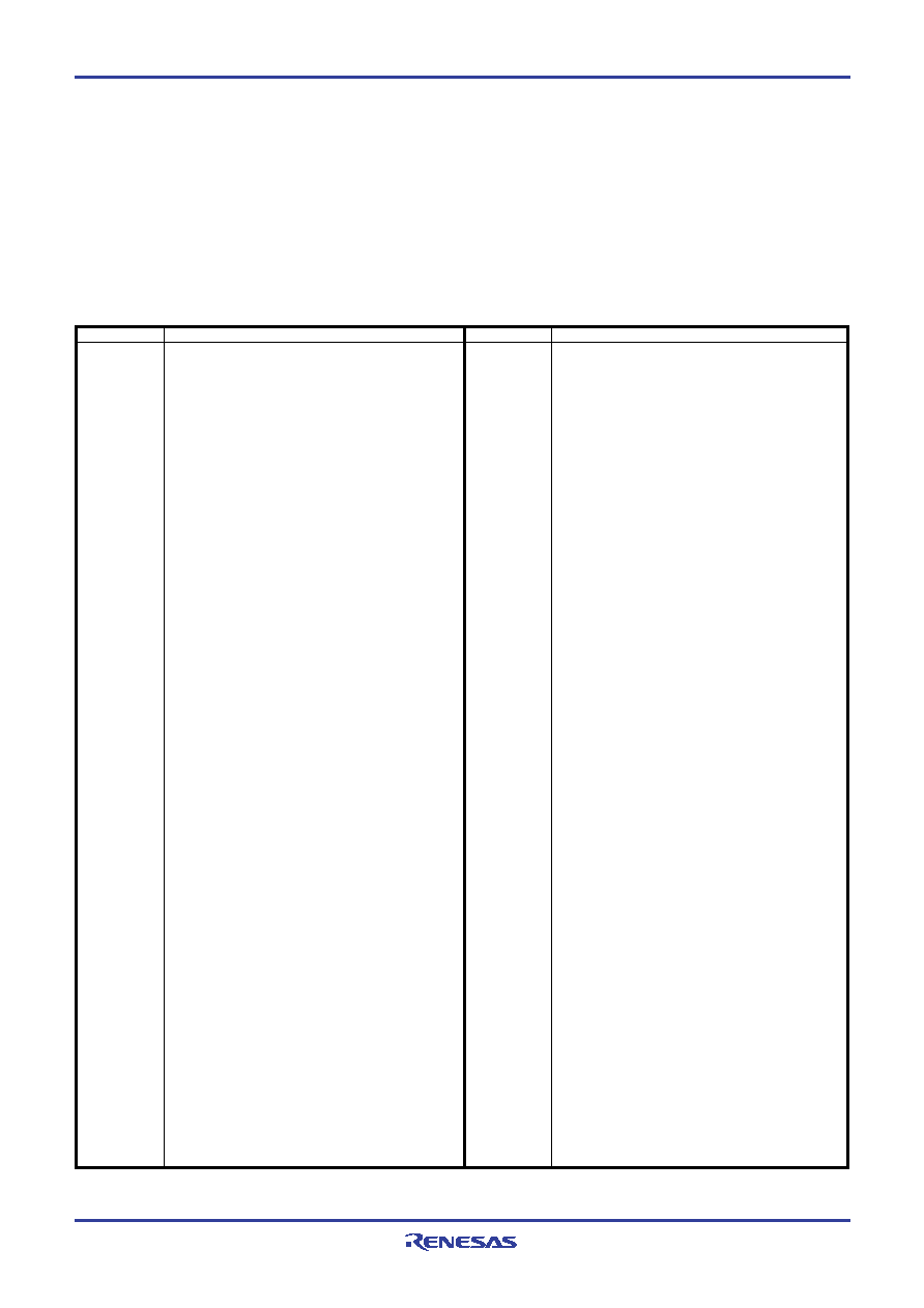
Symbol
A
B
DR
E
V1
V2
I1
MR
RG
PA
W1
W2
W3
W4
L1
L2
L3
C1
C2
PU0
PU1
FR0
FR1
FR2
K0
K1
K2
X
Y
Z
DP
PC
PCH
PCL
SK
SP
CY
UPTF
RPS
R1
R3
R2L
R2H
RLC
Contents
Register A (4 bits)
Register B (4 bits)
Register DR (3 bits)
Register E (8 bits)
Interrupt control register V1 (4 bits)
Interrupt control register V2 (4 bits)
Interrupt control register I1 (4 bits)
Clock control register MR (4 bits)
Clock control register RG (3 bits)
Timer control register PA (1 bit)
Timer control register W1 (4 bits)
Timer control register W2 (4 bits)
Timer control register W3 (4 bits)
Timer control register W4 (4 bits)
LCD control register L1 (4 bits)
LCD control register L2 (4 bits)
LCD control register L3 (4 bits)
LCD control register C1 (4 bits)
LCD control register C2 (4 bits)
Pull-up control register PU0 (4 bits)
Pull-up control register PU1 (4 bits)
Port output structure control register FR0 (4 bits)
Port output structure control register FR1 (4 bits)
Port output structure control register FR2 (4 bits)
Key-on wakeup control register K0 (4 bits)
Key-on wakeup control register K1 (4 bits)
Key-on wakeup control register K2 (4 bits)
Register X (4 bits)
Register Y (4 bits)
Register Z (2 bits)
Data pointer (10 bits)
(It consists of registers X, Y, and Z)
Program counter (14 bits)
High-order 7 bits of program counter
Low-order 7 bits of program counter
Stack register (14 bits 8)
Stack pointer (3 bits)
Carry flag
High-order bit reference enable flag
Prescaler reload register (8 bits)
Timer 1 reload register (8 bits)
Timer 3 reload register (8 bits)
Timer 2 reload register (8 bits)
Timer LC reload register (4 bits)
Contents
Prescaler
Timer 1
Timer 2
Timer 3
Timer LC
Timer 1 interrupt request flag
Timer 2 interrupt request flag
Timer 3 interrupt request flag
Watchdog timer flag
Watchdog timer enable flag
Interrupt enable flag
External 0 interrupt request flag
Power down flag
Port D (8 bits)
Port P0 (4 bits)
Port P1 (4 bits)
Port P2 (4 bits)
Port C (1 bit)
Hexadecimal variable
Hexadecimal constant
Binary notation of hexadecimal variable A
(same for others)
Direction of data movement
Data exchange between a register and memory
Decision of state shown before “?”
Contents of registers and memories
Negate, Flag unchanged after executing instruction
RAM address pointed by the data pointer
Label indicating address a6 a5 a4 a3 a2 a1 a0
in page p6 p5 p4 p3 p2 p1 p0
Hex. C + Hex. number x
Symbol
PS
T1
T2
T3
TLC
T1F
T2F
T3F
WDF1
WEF
INTE
EXF0
P
D
P0
P1
P2
C
x
y
z
p
n
i
j
A3A2A1A0
←
?
( )
—
M(DP)
a
p, a
C
+
x
INSTRUCTIONS
The 4552 Group has the 124 (123) instructions. Each instruction is
described as follows;
(1) Index list of instruction function
(2) Machine instructions (index by alphabet)
(3) Machine instructions (index by function)
(4) Instruction code table
Note : Some instructions of the 4552 Group has the skip function to unexecute the next described instruction. The 4552 Group just invalidates the next instruc-
tion when a skip is performed. The contents of program counter is not increased by 2. Accordingly, the number of cycles does not change even if skip
is not performed. However, the cycle count becomes “1” if the TABP p, RT, or RTS instruction is skipped.
SYMBOL
The symbols shown below are used in the following list of instruc-
tion function and the machine instructions.
相關(guān)PDF資料 |
PDF描述 |
|---|---|
| M34552M8H-XXXFP | 4-BIT, MROM, 6 MHz, MICROCONTROLLER, PQFP48 |
| M34553M4-XXXFP | 4-BIT, MROM, 6 MHz, MICROCONTROLLER, PQFP48 |
| M34553M8H-XXXFP | 4-BIT, MROM, 6 MHz, MICROCONTROLLER, PQFP48 |
| M34554MC-XXXFP | 4-BIT, MROM, 6 MHz, MICROCONTROLLER, PQFP64 |
| M34554EDFP | 4-BIT, OTPROM, 6 MHz, MICROCONTROLLER, PQFP64 |
相關(guān)代理商/技術(shù)參數(shù) |
參數(shù)描述 |
|---|---|
| M34552M8H-XXXFP | 制造商:RENESAS 制造商全稱(chēng):Renesas Technology Corp 功能描述:SINGLE-CHIP 4-BIT CMOS MICROCOMPUTER |
| M34552M8-XXXFP | 制造商:RENESAS 制造商全稱(chēng):Renesas Technology Corp 功能描述:SINGLE-CHIP 4-BIT CMOS MICROCOMPUTER |
| M34552MXH-XXXFP | 制造商:RENESAS 制造商全稱(chēng):Renesas Technology Corp 功能描述:SINGLE-CHIP 4-BIT CMOS MICROCOMPUTER |
| M34552MX-XXXFP | 制造商:RENESAS 制造商全稱(chēng):Renesas Technology Corp 功能描述:SINGLE-CHIP 4-BIT CMOS MICROCOMPUTER |
| M34553G8FP | 制造商:RENESAS 制造商全稱(chēng):Renesas Technology Corp 功能描述:SINGLE-CHIP 4-BIT CMOS MICROCOMPUTER |
發(fā)布緊急采購(gòu),3分鐘左右您將得到回復(fù)。