- 您現(xiàn)在的位置:買賣IC網(wǎng) > PDF目錄370837 > M32000D3FP (Mitsubishi Electric Corporation) SINGLE-CHIP 32-BIT CMOS MICROCOMPUTER PDF資料下載
參數(shù)資料
| 型號(hào): | M32000D3FP |
| 廠商: | Mitsubishi Electric Corporation |
| 英文描述: | SINGLE-CHIP 32-BIT CMOS MICROCOMPUTER |
| 中文描述: | 單芯片32位CMOS微機(jī) |
| 文件頁(yè)數(shù): | 25/45頁(yè) |
| 文件大?。?/td> | 565K |
| 代理商: | M32000D3FP |
第1頁(yè)第2頁(yè)第3頁(yè)第4頁(yè)第5頁(yè)第6頁(yè)第7頁(yè)第8頁(yè)第9頁(yè)第10頁(yè)第11頁(yè)第12頁(yè)第13頁(yè)第14頁(yè)第15頁(yè)第16頁(yè)第17頁(yè)第18頁(yè)第19頁(yè)第20頁(yè)第21頁(yè)第22頁(yè)第23頁(yè)第24頁(yè)當(dāng)前第25頁(yè)第26頁(yè)第27頁(yè)第28頁(yè)第29頁(yè)第30頁(yè)第31頁(yè)第32頁(yè)第33頁(yè)第34頁(yè)第35頁(yè)第36頁(yè)第37頁(yè)第38頁(yè)第39頁(yè)第40頁(yè)第41頁(yè)第42頁(yè)第43頁(yè)第44頁(yè)第45頁(yè)
SINGLE-CHIP 32-BIT CMOS MICROCOMPUTER
MITSUBISHI MICROCOMPUTERS
M32000D3FP
25
("L" output)
("L" output)
("L" output)
"Hi-z"
"Hi-z"
"Hi-z"
"Hi-z"
"Hi-z"
"Hi-z"
"Hi-z"
"Hi-z"
"Hi-z"
"Hi-z"
"Hi-z"
"Hi-z"
8
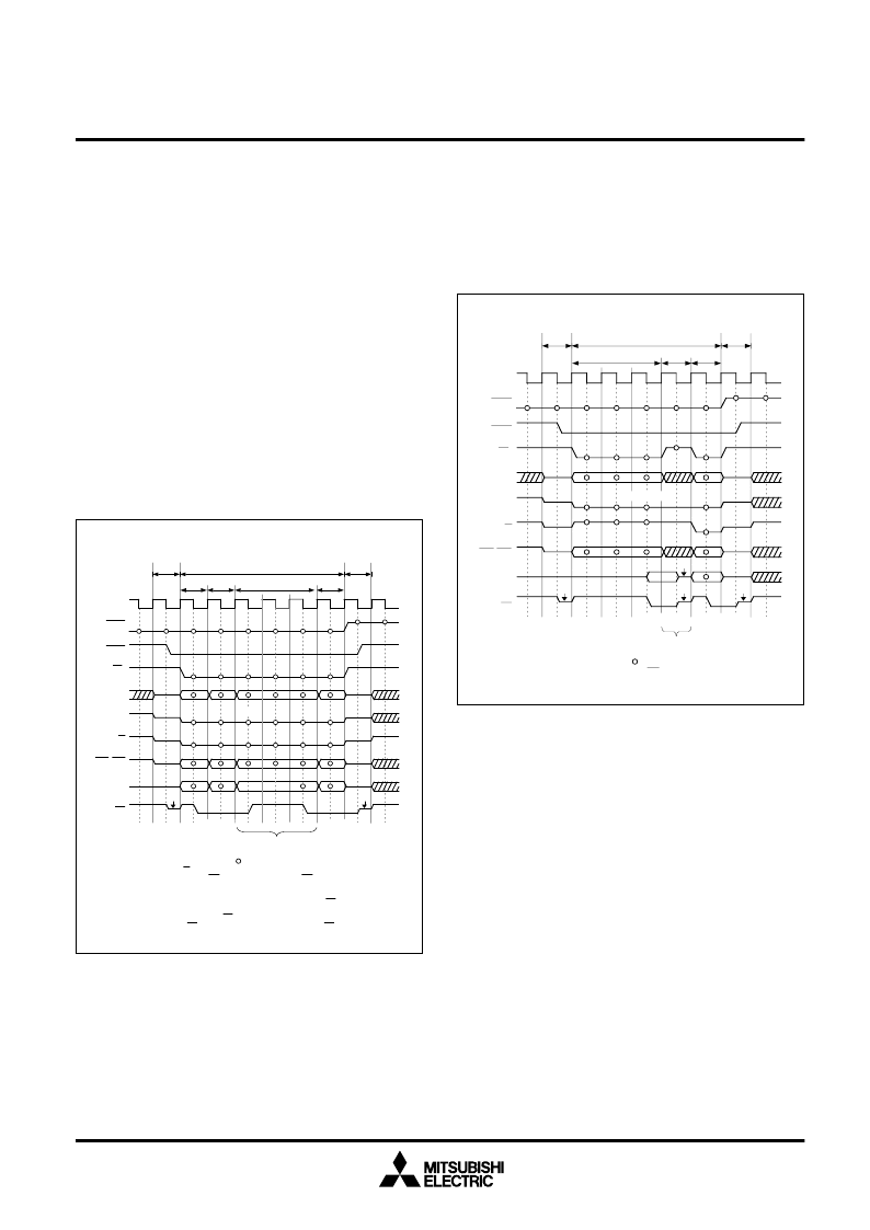
CLKIN
HREQ
BCH, BCL
D0 - D15
DC
R/W
hold shift
hold
return
HACK
A8 - A30
CS
write
write
write
write
SID
Note:
"Hi-z" means high impedance, and indicates sampling timing.
The value of the R/W signal that controls the data direction of the bus interface
8
, 3 to 7 CLKIN clock periods are necessary for writing
operation to internal DRAM crossing an 128-bit boundary. Hold the input value of the
address or other control signals during these wait cycle periods (DC = "H"). Consecutive
writing operations within an 128-bit boundary are completed in 1 CLKIN clock period.
When the M32000D3FP is in the hold state and an "L" level is input
to CS, the M32000D3FP interprets it as a bus access request to the
internal DRAM. In this case, when the R/W signal is at an "L" level,
the memory controller drives a write cycle to the internal DRAM. Byte
data control is specified by the BCH and BCL signals. Only data in
the byte positions for which an "L" level is input to BCH or BCL are
written. When writing is complete, an "L" level DC signal is output.
The M32000D3FP stores the requested data in the 128-bit data buffer
of the BIU, before writing to the internal DRAM. This reduces the
number of accesses to the internal DRAM when a request to writing
to consecutive addresses is made, and improves bus cycle through-
put. Consecutive write cycles within an 128-bit boundary are com-
pleted in 1 CLKIN clock period. 3 to 7 CLKIN clock periods are nec-
essary for a write access crossing an 128-bit boundary when writing
to the internal DRAM. After DC outputs an "L" level (access com-
plete), return CS to the "H" level between the CLKIN falling edge
corresponding to the last write cycle and the following CLKIN falling
edge. Return HREQ to the "H" level to return the M32000D3FP to
the normal operation mode from the hold state either at the same
time as or after CS is returned to the "H" level.
When the external bus master makes an access, the value of the
R/W signal that controls the data direction of the bus interface can-
not be changed during CS="L". Therefore, read cycles and write cycles
cannot be mixed while CS = "L". When starting a write cycle follow-
ing after a read cycle and starting a read cycle following a write cycle,
keep the CS signal at an "H" level for at least 1 CLKIN.
Fig. 24 Write bus cycle to internal DRAM
Fig. 25 Read/write bus cycle
CLKIN
HREQ
BCH, BCL
D0 - D15
DC
R/W
hold shift
hold
return
HACK
A8 - A30
CS
("L" output)
read
CS = "H"
write
("L" output)
SID
("L" input)
"Hi-z"
"Hi-z"
"Hi-z"
"Hi-z"
"Hi-z"
"Hi-z"
"Hi-z"
"Hi-z"
"Hi-z"
"Hi-z"
"Hi-z"
8
"Hi-z"
"Hi-z"
Note:
"Hi-z" means high-impedance, and indicates sampling timing.
Also, where marked above with
8
, keep CS signal to "H" at least 1 CLKIN when
starting a write bus cycle after a read bus cycle or a read bus cycle after a write
"Hi-z"
相關(guān)PDF資料 |
PDF描述 |
|---|---|
| M32000D4 | SINGLE CHIP 32 BIT CMOS MICROCOMPUTER |
| M32000D4AFP | SINGLE CHIP 32 BIT CMOS MICROCOMPUTER |
| M32170F3VFP | SINGLE-CHIP 32-BIT CMOS MICROCOMPUTER |
| M32174F3VFP | SINGLE-CHIP 32-BIT CMOS MICROCOMPUTER |
| M32170F3VFG | 32-BIT RISC SINGLE-CHIP MICROCOMPUTER |
相關(guān)代理商/技術(shù)參數(shù) |
參數(shù)描述 |
|---|---|
| M32000D4 | 制造商:MITSUBISHI 制造商全稱:Mitsubishi Electric Semiconductor 功能描述:SINGLE CHIP 32 BIT CMOS MICROCOMPUTER |
| M32000D4AFP | 制造商:MITSUBISHI 制造商全稱:Mitsubishi Electric Semiconductor 功能描述:SINGLE CHIP 32 BIT CMOS MICROCOMPUTER |
| M32000D4BFP-80 | 制造商:MITSUBISHI 制造商全稱:Mitsubishi Electric Semiconductor 功能描述:SINGLE-CHIP 32-BIT CMOS MICROCOMPUTER |
| M32002AGLJ | 制造商:MTRONPTI 制造商全稱:MTRONPTI 功能描述:9x14 mm, 3.3/2.5/1.8 Volt, PECL/LVDS/CML, VCXO |
| M32002AGMJ | 制造商:MTRONPTI 制造商全稱:MTRONPTI 功能描述:9x14 mm, 3.3/2.5/1.8 Volt, PECL/LVDS/CML, VCXO |
發(fā)布緊急采購(gòu),3分鐘左右您將得到回復(fù)。