- 您現(xiàn)在的位置:買賣IC網(wǎng) > PDF目錄45018 > M30627MHP-XXXGP 16-BIT, MROM, 24 MHz, MICROCONTROLLER, PQFP128 PDF資料下載
參數(shù)資料
| 型號: | M30627MHP-XXXGP |
| 元件分類: | 微控制器/微處理器 |
| 英文描述: | 16-BIT, MROM, 24 MHz, MICROCONTROLLER, PQFP128 |
| 封裝: | 14 X 20 MM, 0.50 MM PITCH, PLASTIC, LQFP-128 |
| 文件頁數(shù): | 108/348頁 |
| 文件大小: | 4209K |
| 代理商: | M30627MHP-XXXGP |
第1頁第2頁第3頁第4頁第5頁第6頁第7頁第8頁第9頁第10頁第11頁第12頁第13頁第14頁第15頁第16頁第17頁第18頁第19頁第20頁第21頁第22頁第23頁第24頁第25頁第26頁第27頁第28頁第29頁第30頁第31頁第32頁第33頁第34頁第35頁第36頁第37頁第38頁第39頁第40頁第41頁第42頁第43頁第44頁第45頁第46頁第47頁第48頁第49頁第50頁第51頁第52頁第53頁第54頁第55頁第56頁第57頁第58頁第59頁第60頁第61頁第62頁第63頁第64頁第65頁第66頁第67頁第68頁第69頁第70頁第71頁第72頁第73頁第74頁第75頁第76頁第77頁第78頁第79頁第80頁第81頁第82頁第83頁第84頁第85頁第86頁第87頁第88頁第89頁第90頁第91頁第92頁第93頁第94頁第95頁第96頁第97頁第98頁第99頁第100頁第101頁第102頁第103頁第104頁第105頁第106頁第107頁當(dāng)前第108頁第109頁第110頁第111頁第112頁第113頁第114頁第115頁第116頁第117頁第118頁第119頁第120頁第121頁第122頁第123頁第124頁第125頁第126頁第127頁第128頁第129頁第130頁第131頁第132頁第133頁第134頁第135頁第136頁第137頁第138頁第139頁第140頁第141頁第142頁第143頁第144頁第145頁第146頁第147頁第148頁第149頁第150頁第151頁第152頁第153頁第154頁第155頁第156頁第157頁第158頁第159頁第160頁第161頁第162頁第163頁第164頁第165頁第166頁第167頁第168頁第169頁第170頁第171頁第172頁第173頁第174頁第175頁第176頁第177頁第178頁第179頁第180頁第181頁第182頁第183頁第184頁第185頁第186頁第187頁第188頁第189頁第190頁第191頁第192頁第193頁第194頁第195頁第196頁第197頁第198頁第199頁第200頁第201頁第202頁第203頁第204頁第205頁第206頁第207頁第208頁第209頁第210頁第211頁第212頁第213頁第214頁第215頁第216頁第217頁第218頁第219頁第220頁第221頁第222頁第223頁第224頁第225頁第226頁第227頁第228頁第229頁第230頁第231頁第232頁第233頁第234頁第235頁第236頁第237頁第238頁第239頁第240頁第241頁第242頁第243頁第244頁第245頁第246頁第247頁第248頁第249頁第250頁第251頁第252頁第253頁第254頁第255頁第256頁第257頁第258頁第259頁第260頁第261頁第262頁第263頁第264頁第265頁第266頁第267頁第268頁第269頁第270頁第271頁第272頁第273頁第274頁第275頁第276頁第277頁第278頁第279頁第280頁第281頁第282頁第283頁第284頁第285頁第286頁第287頁第288頁第289頁第290頁第291頁第292頁第293頁第294頁第295頁第296頁第297頁第298頁第299頁第300頁第301頁第302頁第303頁第304頁第305頁第306頁第307頁第308頁第309頁第310頁第311頁第312頁第313頁第314頁第315頁第316頁第317頁第318頁第319頁第320頁第321頁第322頁第323頁第324頁第325頁第326頁第327頁第328頁第329頁第330頁第331頁第332頁第333頁第334頁第335頁第336頁第337頁第338頁第339頁第340頁第341頁第342頁第343頁第344頁第345頁第346頁第347頁第348頁
Mitsubishi microcomputers
M16C / 62P Group
SINGLE-CHIP 16-BIT CMOS MICROCOMPUTER
A-D Converter
196
Under
development
Preliminary Specifications Rev.1.0
Specifications in this manual are tentative and subject to change.
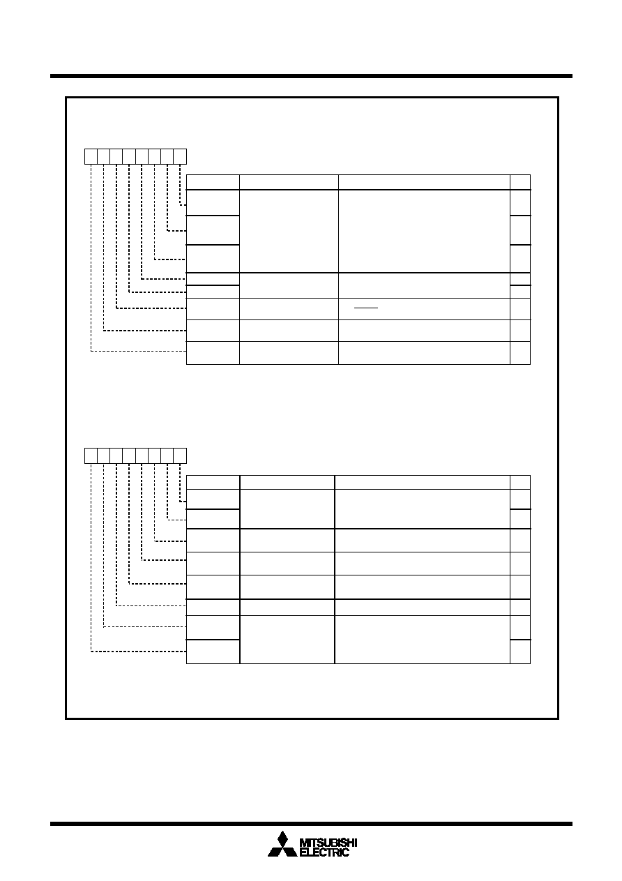
A-D control register 0 (Note 1)
Symbol
Address
After reset
ADCON0
03D616
00000XXX2
b7
b6
b5
b4
b3
b2
b1
b0
Analog input pin
select bit
CH0
Bit symbol
Bit name
Function
CH1
CH2
A-D operation mode
select bit 0
MD0
MD1
Trigger select bit
0 : Software trigger
1 : ADTRG trigger
TRG
ADST
A-D conversion start flag
0 : A-D conversion disabled
1 : A-D conversion started
Frequency select bit 0
CKS0
RW
A-D control register 1 (Note)
Symbol
Address
After reset
ADCON1
03D716
0016
Bit name
Function
Bit symbol
b7
b6
b5
b4
b3
b2
b1
b0
A-D sweep pin
select bit
SCAN0
SCAN1
MD2
BITS
8/10-bit mode select bit
0 : 8-bit mode
1 : 10-bit mode
VCUT
OPA0
Vref connect bit (Note 2)
OPA1
A-D operation mode
select bit 1
1 : Vref connected
External op-amp
connection mode bit
01
Invalid in repeat mode
0
0 0 0 : AN0 is selected
0 0 1 : AN1 is selected
0 1 0 : AN2 is selected
0 1 1 : AN3 is selected
1 0 0 : AN4 is selected
1 0 1 : AN5 is selected
1 1 0 : AN6 is selected
(Note 2)
1 1 1 : AN7 is selected
(Note 3)
b2 b1 b0
0 1 : Repeat mode
(Note 3)
b4 b3
0 0 : ANEX0 and ANEX1 are not used
0 1 : ANEX0 input is A-D converted
1 0 : ANEX1 input is A-D converted
1 1 : External op-amp connection mode
b7 b6
1
Frequency select bit 1
CKS1
Set to “0” when this mode is selected
RW
See Note 3 for the ADCON2 register
Note 1: If the ADCON0 register is rewritten during A-D conversion, the conversion result will be indeterminate.
Note 2: AN00 to AN07, and AN20 to AN27 can be used in the same way as AN0 to AN7. Use the ADCON2 register’s
ADGSEL1 to ADGSEL0 bits to select the desired pin. However, if VCC2 < VCC1, do not use AN00 to AN07 and
AN20 to AN27 as analog input pins.
Note 3: After rewriting the MD1 to MD0 bits, set the CH2 to CH0 bits over again using another instruction.
Note 1: If the ADCON1 register is rewritten during A-D conversion, the conversion result will be indeterminate.
Note 2: If the VCUT bit is reset from “0” (Vref unconnected) to “1” (Vref connected), wait for 1 s or more before starting
A-D conversion.
See Note 3 for the ADCON2 register
Figure 1.22.5. ADCON0 Register and ADCON1 Register (Repeat Mode)
相關(guān)PDF資料 |
PDF描述 |
|---|---|
| M30626FHPFP | 16-BIT, FLASH, 24 MHz, MICROCONTROLLER, PQFP100 |
| M30623MWP-XXXGP | 16-BIT, MROM, 24 MHz, MICROCONTROLLER, PQFP128 |
| M30626MWP-XXXFP | 16-BIT, MROM, 24 MHz, MICROCONTROLLER, PQFP100 |
| M30620SPGP | 16-BIT, 24 MHz, MICROCONTROLLER, PQFP100 |
| M30622MEP-XXXGP | 16-BIT, MROM, 24 MHz, MICROCONTROLLER, PQFP100 |
相關(guān)代理商/技術(shù)參數(shù) |
參數(shù)描述 |
|---|---|
| M30627MJP-XXXGP | 制造商:RENESAS 制造商全稱:Renesas Technology Corp 功能描述:SINGLE-CHIP 16-BIT CMOS MICROCOMPUTER |
| M30627MWP | 制造商:RENESAS 制造商全稱:Renesas Technology Corp 功能描述:SINGLE-CHIP 16-BIT CMOS MICROCOMPUTER |
| M30627MWP-XXXGP | 制造商:RENESAS 制造商全稱:Renesas Technology Corp 功能描述:SINGLE-CHIP 16-BIT CMOS MICROCOMPUTER |
| M3062AFCTFP | 制造商:RENESAS 制造商全稱:Renesas Technology Corp 功能描述:SINGLE-CHIP 16-BIT CMOS MICROCOMPUTER |
| M3062AFCTGP | 制造商:RENESAS 制造商全稱:Renesas Technology Corp 功能描述:SINGLE-CHIP 16-BIT CMOS MICROCOMPUTER |
發(fā)布緊急采購,3分鐘左右您將得到回復(fù)。