- 您現(xiàn)在的位置:買賣IC網(wǎng) > PDF目錄370836 > M30623MAH-A81GP (Mitsubishi Electric Corporation) SINGLE-CHIP 16-BIT CMOS MICROCOMPUTER PDF資料下載
參數(shù)資料
| 型號: | M30623MAH-A81GP |
| 廠商: | Mitsubishi Electric Corporation |
| 英文描述: | SINGLE-CHIP 16-BIT CMOS MICROCOMPUTER |
| 中文描述: | 單片16位CMOS微機(jī) |
| 文件頁數(shù): | 43/184頁 |
| 文件大小: | 1734K |
| 代理商: | M30623MAH-A81GP |
第1頁第2頁第3頁第4頁第5頁第6頁第7頁第8頁第9頁第10頁第11頁第12頁第13頁第14頁第15頁第16頁第17頁第18頁第19頁第20頁第21頁第22頁第23頁第24頁第25頁第26頁第27頁第28頁第29頁第30頁第31頁第32頁第33頁第34頁第35頁第36頁第37頁第38頁第39頁第40頁第41頁第42頁當(dāng)前第43頁第44頁第45頁第46頁第47頁第48頁第49頁第50頁第51頁第52頁第53頁第54頁第55頁第56頁第57頁第58頁第59頁第60頁第61頁第62頁第63頁第64頁第65頁第66頁第67頁第68頁第69頁第70頁第71頁第72頁第73頁第74頁第75頁第76頁第77頁第78頁第79頁第80頁第81頁第82頁第83頁第84頁第85頁第86頁第87頁第88頁第89頁第90頁第91頁第92頁第93頁第94頁第95頁第96頁第97頁第98頁第99頁第100頁第101頁第102頁第103頁第104頁第105頁第106頁第107頁第108頁第109頁第110頁第111頁第112頁第113頁第114頁第115頁第116頁第117頁第118頁第119頁第120頁第121頁第122頁第123頁第124頁第125頁第126頁第127頁第128頁第129頁第130頁第131頁第132頁第133頁第134頁第135頁第136頁第137頁第138頁第139頁第140頁第141頁第142頁第143頁第144頁第145頁第146頁第147頁第148頁第149頁第150頁第151頁第152頁第153頁第154頁第155頁第156頁第157頁第158頁第159頁第160頁第161頁第162頁第163頁第164頁第165頁第166頁第167頁第168頁第169頁第170頁第171頁第172頁第173頁第174頁第175頁第176頁第177頁第178頁第179頁第180頁第181頁第182頁第183頁第184頁
43
Tentative Specifications REV.A
S
pecifications in this manual are tentative and subject to change.
Clock Generating Circuit
Mitsubishi microcomputers
M16C / 62T Group
SINGLE-CHIP 16-BIT CMOS MICROCOMPUTER
deveopmen
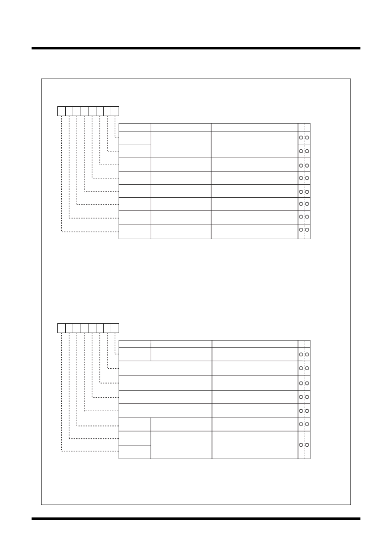
Figure 1.13.4 shows the system clock control registers 0 and 1.
Figure 1.13.4. Clock control registers 0 and 1
System clock control register 0 (Note 1)
Symbol
CM0
Address
0006
16
When reset
48
16
Bit name
Function
Bit symbol
b7
b6
b5
b4
b3
b2
b1
b0
0 0 : I/O port P5
7
0 1 : f
C
output
1 0 : f
8
output
1 1 : f
32
output
0 : Do not stop f
1
, f
8
, f
32
in wait mode
1 : Stop f
1
, f
8
, f
32
in wait mode
0 : LOW
1 : HIGH
b1 b0
CM07
CM05
CM04
CM03
CM01
CM02
CM00
CM06
Clock output function
select bit
WAIT peripheral function
clock stop bit
X
CIN
-X
COUT
drive capacity
select bit (Note 2)
Port X
C
select bit
0 : I/O port
1 : X
CIN
-X
COUT
generation
0 : On
1 : Off
0 : CM16 and CM17 valid
1 : Division by 8 mode
Main clock (X
IN
-X
OUT
)
stop bit (Note 4) (Note 5)
Main clock division select
bit 0 (Note 2)
System clock select bit
(Note 6)
0 : X
IN
, X
OUT
1 : X
CIN
, X
COUT
Note 1: Set bit 0 of the protect register (address 000A
16
) to “1” before writing to this register.
Note 2: Changes to “1” when shiffing to stop mode.
Note 3: When entering power saving mode, main clock stops using this bit. When returning from stop
mode and operating with X
IN
, set this bit to “0”. When main clock oscillation is operating by
itself, set system clock select bit (CM07) to “1” before setting this bit to “1”.
Note 4: When inputting external clock, only clock oscillation buffer is stopped and clock input is acceptable.
Note 5: If this bit is set to “1”, X
OUT
turns “H”. The built-in feedback resistor remains ON, so X
IN
turns pulled
up to X
OUT
(“H”) via the feedback resistor.
Note 6: Set port Xc select bit (CM04) to “1” before writing to this bit. The both bits can not be written at
the same time.
System clock control register 1 (Note 1)
Symbol
CM1
Address
0007
16
When reset
20
16
Bit name
Function
Bit symbol
b7
b6
b5
b4
0
b3
0
b2
0
b1
0
b0
CM10
All clock stop control bit
(Note4)
0 : Clock on
1 : All clocks off (stop mode)
Note 1: Set bit 0 of the protect register (address 000A
16
) to
“1” before writing to this register.
Note 2: Changes to
“1” when shiffing to stop mode.
Note 3: Can be selected when bit 6 of the system clock control register 0 (address 0006
16
) is
“0”.
If
“1”, division mode is fixed at 8.
Note 4: If this bit is set to “1”, X
OUT
turns “H”, and the built-in feedback resistor turns null.
CM15
X
IN
-X
OUT
drive capacity
select bit (Note 2)
0 : LOW
1 : HIGH
W
R
CM16
CM17
Reserved bit
Always set to
“0”
Reserved bit
Always set to
“0”
Main clock division
select bit 1 (Note 3)
0 1 : Division by 2 mode
1 0 : Division by 4 mode
1 1 : Division by 16 mode
b7 b6
Reserved bit
Always set to
“0”
Reserved bit
Always set to
“0”
AA
AA
AA
AA
AA
AA
AA
AA
AA
AA
AA
AA
AA
AA
AA
AA
相關(guān)PDF資料 |
PDF描述 |
|---|---|
| M30623ECTGP | SINGLE-CHIP 16-BIT CMOS MICROCOMPUTER |
| M30623M4 | SINGLE-CHIP 16-BIT CMOS MICROCOMPUTER |
| M30623M4T-243GP | SINGLE-CHIP 16-BIT CMOS MICROCOMPUTER |
| M30623M4T-245GP | SINGLE-CHIP 16-BIT CMOS MICROCOMPUTER |
| M30623MAA-2ATGP | SINGLE-CHIP 16-BIT CMOS MICROCOMPUTER |
相關(guān)代理商/技術(shù)參數(shù) |
參數(shù)描述 |
|---|---|
| M30623MAP | 制造商:RENESAS 制造商全稱:Renesas Technology Corp 功能描述:SINGLE-CHIP 16-BIT CMOS MICROCOMPUTER |
| M30623MAP-XXXGP | 制造商:RENESAS 制造商全稱:Renesas Technology Corp 功能描述:SINGLE-CHIP 16-BIT CMOS MICROCOMPUTER |
| M30623MA-XXXGP | 制造商:RENESAS 制造商全稱:Renesas Technology Corp 功能描述:SINGLE-CHIP 16-BIT CMOS MICROCOMPUTER |
| M30623MC | 制造商:RENESAS 制造商全稱:Renesas Technology Corp 功能描述:SINGLE-CHIP 16-BIT CMOS MICROCOMPUTER |
| M30623MCA-B72GP | 制造商:MITSUBISHI 制造商全稱:Mitsubishi Electric Semiconductor 功能描述:SINGLE-CHIP 16-BIT CMOS MICROCOMPUTER |
發(fā)布緊急采購,3分鐘左右您將得到回復(fù)。