- 您現(xiàn)在的位置:買賣IC網(wǎng) > PDF目錄370833 > M30612M8A (Mitsubishi Electric Corporation) SINGLE-CHIP 16-BIT CMOS MICROCOMPUTER PDF資料下載
參數(shù)資料
| 型號: | M30612M8A |
| 廠商: | Mitsubishi Electric Corporation |
| 英文描述: | SINGLE-CHIP 16-BIT CMOS MICROCOMPUTER |
| 中文描述: | 單片16位CMOS微機(jī) |
| 文件頁數(shù): | 150/197頁 |
| 文件大?。?/td> | 2673K |
| 代理商: | M30612M8A |
第1頁第2頁第3頁第4頁第5頁第6頁第7頁第8頁第9頁第10頁第11頁第12頁第13頁第14頁第15頁第16頁第17頁第18頁第19頁第20頁第21頁第22頁第23頁第24頁第25頁第26頁第27頁第28頁第29頁第30頁第31頁第32頁第33頁第34頁第35頁第36頁第37頁第38頁第39頁第40頁第41頁第42頁第43頁第44頁第45頁第46頁第47頁第48頁第49頁第50頁第51頁第52頁第53頁第54頁第55頁第56頁第57頁第58頁第59頁第60頁第61頁第62頁第63頁第64頁第65頁第66頁第67頁第68頁第69頁第70頁第71頁第72頁第73頁第74頁第75頁第76頁第77頁第78頁第79頁第80頁第81頁第82頁第83頁第84頁第85頁第86頁第87頁第88頁第89頁第90頁第91頁第92頁第93頁第94頁第95頁第96頁第97頁第98頁第99頁第100頁第101頁第102頁第103頁第104頁第105頁第106頁第107頁第108頁第109頁第110頁第111頁第112頁第113頁第114頁第115頁第116頁第117頁第118頁第119頁第120頁第121頁第122頁第123頁第124頁第125頁第126頁第127頁第128頁第129頁第130頁第131頁第132頁第133頁第134頁第135頁第136頁第137頁第138頁第139頁第140頁第141頁第142頁第143頁第144頁第145頁第146頁第147頁第148頁第149頁當(dāng)前第150頁第151頁第152頁第153頁第154頁第155頁第156頁第157頁第158頁第159頁第160頁第161頁第162頁第163頁第164頁第165頁第166頁第167頁第168頁第169頁第170頁第171頁第172頁第173頁第174頁第175頁第176頁第177頁第178頁第179頁第180頁第181頁第182頁第183頁第184頁第185頁第186頁第187頁第188頁第189頁第190頁第191頁第192頁第193頁第194頁第195頁第196頁第197頁
Mitsubishi microcomputers
M16C / 61 Group
SINGLE-CHIP 16-BIT CMOS MICROCOMPUTER
Timing (Vcc = 5V)
150
Symbol
Standard
Min.
Measuring condition
Max.
25
Parameter
Unit
t
d(BCLK-AD)
t
h(BCLK-AD)
t
h(RD-AD)
t
h(WR-AD)
Address output delay time
Address output hold time (BCLK standard)
Address output hold time (RD standard)
Address output hold time (WR standard)
ns
ns
ns
ns
4
0
0
t
h(BCLK-CS)
t
d(BCLK-ALE)
t
h(BCLK-ALE)
t
d(BCLK-RD)
t
h(BCLK-RD)
t
d(BCLK-WR)
t
h(BCLK-WR)
t
d(BCLK-DB)
t
h(BCLK-DB)
t
d(DB-WR)
Chip select output hold time (BCLK standard)
ALE signal output delay time
ALE signal output hold time
RD signal output delay time
RD signal output hold time
WR signal output delay time
WR signal output hold time
Data output delay time (BCLK standard)
Data output hold time (BCLK standard)
Data output delay time (WR standard)
4
ns
ns
ns
ns
ns
ns
ns
ns
ns
ns
25
– 4
25
0
25
0
40
4
t
h(WR-DB)
Note 1: Calculated according to the BCLK frequency as follows:
10
9
Data output hold time (WR standard)(Note2)
0
ns
(Note1)
td(DB – WR) =
f(BCLK) X 2
– 40
[ns]
t
d(BCLK-CS)
Chip select output delay time
25
ns
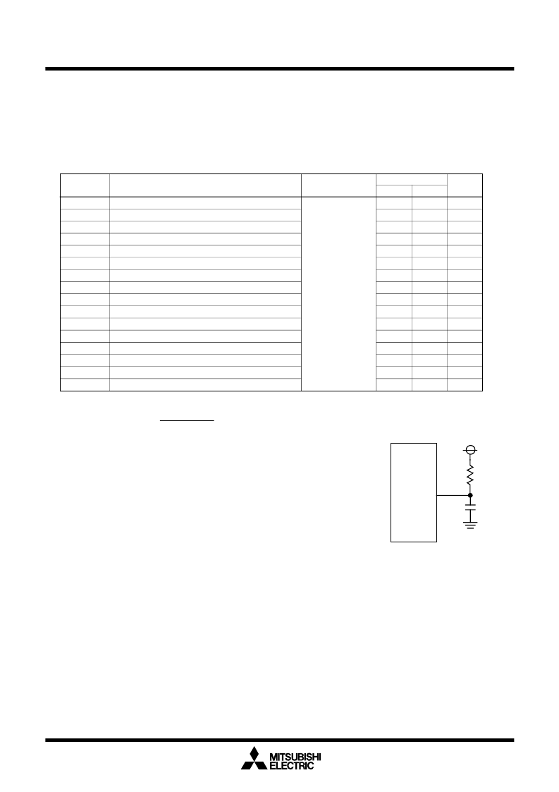
Note 2: This is standard value shows the timing when the output is off,
and doesn't show hold time of data bus.
Hold time of data bus is different by capacitor volume and pull-up
(pull-down) resistance value.
Hold time of data bus is expressed in
t = –CR X ln (1 – V
OL
/ V
CC
)
by a circuit of the right figure.
For example, when V
OL
= 0.2V
CC
, C = 30pF, R = 1k
, hold time
of output “L” level is
t = – 30pF X 1k
X ln (1 – 0.2V
CC
/ V
CC
)
= 6.7ns.
DBi
R
C
Switching characteristics (referenced to V
CC
= 5V, V
SS
= 0V at Ta = 25
o
C, CM15 = “1” unless
otherwise specified)
V
CC
= 5V
Figure
1.24.1
Table 1.24.19. Memory expansion mode and microprocessor mode (no wait)
發(fā)布緊急采購,3分鐘左右您將得到回復(fù)。