- 您現(xiàn)在的位置:買(mǎi)賣(mài)IC網(wǎng) > PDF目錄45010 > M30240MC-XXXFP 16-BIT, MROM, MICROCONTROLLER, PQFP80 PDF資料下載
參數(shù)資料
| 型號(hào): | M30240MC-XXXFP |
| 元件分類(lèi): | 微控制器/微處理器 |
| 英文描述: | 16-BIT, MROM, MICROCONTROLLER, PQFP80 |
| 封裝: | 0.80 MM PITCH, PLASTIC, QFP-80 |
| 文件頁(yè)數(shù): | 68/125頁(yè) |
| 文件大?。?/td> | 753K |
| 代理商: | M30240MC-XXXFP |
第1頁(yè)第2頁(yè)第3頁(yè)第4頁(yè)第5頁(yè)第6頁(yè)第7頁(yè)第8頁(yè)第9頁(yè)第10頁(yè)第11頁(yè)第12頁(yè)第13頁(yè)第14頁(yè)第15頁(yè)第16頁(yè)第17頁(yè)第18頁(yè)第19頁(yè)第20頁(yè)第21頁(yè)第22頁(yè)第23頁(yè)第24頁(yè)第25頁(yè)第26頁(yè)第27頁(yè)第28頁(yè)第29頁(yè)第30頁(yè)第31頁(yè)第32頁(yè)第33頁(yè)第34頁(yè)第35頁(yè)第36頁(yè)第37頁(yè)第38頁(yè)第39頁(yè)第40頁(yè)第41頁(yè)第42頁(yè)第43頁(yè)第44頁(yè)第45頁(yè)第46頁(yè)第47頁(yè)第48頁(yè)第49頁(yè)第50頁(yè)第51頁(yè)第52頁(yè)第53頁(yè)第54頁(yè)第55頁(yè)第56頁(yè)第57頁(yè)第58頁(yè)第59頁(yè)第60頁(yè)第61頁(yè)第62頁(yè)第63頁(yè)第64頁(yè)第65頁(yè)第66頁(yè)第67頁(yè)當(dāng)前第68頁(yè)第69頁(yè)第70頁(yè)第71頁(yè)第72頁(yè)第73頁(yè)第74頁(yè)第75頁(yè)第76頁(yè)第77頁(yè)第78頁(yè)第79頁(yè)第80頁(yè)第81頁(yè)第82頁(yè)第83頁(yè)第84頁(yè)第85頁(yè)第86頁(yè)第87頁(yè)第88頁(yè)第89頁(yè)第90頁(yè)第91頁(yè)第92頁(yè)第93頁(yè)第94頁(yè)第95頁(yè)第96頁(yè)第97頁(yè)第98頁(yè)第99頁(yè)第100頁(yè)第101頁(yè)第102頁(yè)第103頁(yè)第104頁(yè)第105頁(yè)第106頁(yè)第107頁(yè)第108頁(yè)第109頁(yè)第110頁(yè)第111頁(yè)第112頁(yè)第113頁(yè)第114頁(yè)第115頁(yè)第116頁(yè)第117頁(yè)第118頁(yè)第119頁(yè)第120頁(yè)第121頁(yè)第122頁(yè)第123頁(yè)第124頁(yè)第125頁(yè)
Mitsubishi microcomputers
M16C / 24 Group
SINGLE-CHIP 16-BIT CMOS MICROCOMPUTER
49
CONFIDENTIAL
Preliminary Specifications REV.B
Specifications in this manual are tentative and subject to change
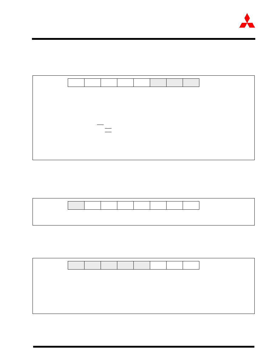
Universal Serial Bus
The USB Control Register, shown in Figure 31, is used to control the USB FCU (for Microsoft Legacy
Application, please see Addendum). This register is not reset by a USB reset signaling. After the USB
is enabled (USBC7 set to “1”), a minimum delay of 250ns (three 12 MHz clock periods) is needed be-
fore performing any other USB register read/write operations.
Figure 31:
USB Control Register (for Microsoft Legacy Application, see Addendum)
The USB Function Address Register, shown in Figure 32, maintains the 7-bit USB address assigned
by the host. The USB FCU uses this register value to decode USB token packet addresses. At reset,
when the device is not yet configured, the value is 0016.
Figure 32:
USB Function Address Register
The USB Power Management Register, shown in Figure 33, is used for power management in the
USB FCU.
Figure 33:
USB Power Management Register
Bit 2:0
Reserved
USBC3
Transceiver Voltage Converter High/Low Current Mode Selection Bit (bit 3)
0: High current mode, for USB normal operation
1: Low current mode, for USB suspend operation
USBC4
USB Transceiver Voltage Converter Enable Bit (bit 4)
0: USB transceiver voltage converter disabled
1: USB transceiver voltage converter enabled
USBC5
USB Clock Enable Bit (bit 5)
0: 48 MHz clock to the USB block is disabled.
1: 48 MHz clock to the USB block is enabled.
USBC6
USB SOF Port Select Bit (bit 6)
0: USB SOF output is disabled. P86 is used as GPIO pin.
1: USB SOF output is enabled
USBC7
USB Enable Bit (bit 7)
0: USB block is disabled, all USB internal registers are held at their default values.
1: USB block is enabled
MSB
7
LSB
0
USBC7
USBC6
USBC5
USBC4
USBC3
Reserved Reserved
Access: R/W
Reset:
0016
Address: 000C16
Reserved
FUNAD6:0
7-bit programmable Function Address (bits 6-0)
Bit 7
Reserved (Read/Write “0”)
MSB
7
LSB
0
Reserved
FUNAD6
FUNAD5
FUNAD4
FUNAD3
FUNAD1
FUNAD0
Access: R/W
Reset:
0016
FUNAD2
Address: 030016
SUSPEND
USB Suspend Detection Flag (bit 0) (Write “0” only or Read)
0: No USB suspend signal detected
1: USB suspend signal detected
RESUME
USB Resume Detection Flag (bit 1) (Write “0” only or Read)
0: No USB resume signal detected
1: USB resume signal detected
WAKEUP
USB Remote Wake-up Bit (bit 2)
0: End remote resume signaling
1: Remote resume signaling (If SUSPEND = “1”)
Bit7:3
Reserved (Read/Write “0”)
MSB
7
LSB
0
Reserved Reserved Reserved Reserved Reserved
RESUME SUSPEND
Access: R/W
Reset:
0016
WAKEUP
Address: 030116
相關(guān)PDF資料 |
PDF描述 |
|---|---|
| M30240M4-XXXFP | 16-BIT, MROM, MICROCONTROLLER, PQFP80 |
| M30240M1-XXXFP | 16-BIT, MROM, MICROCONTROLLER, PQFP80 |
| M30245MC-XXXGP | 16-BIT, MROM, 16 MHz, MICROCONTROLLER, PQFP100 |
| M30245FCGP | 16-BIT, FLASH, 16 MHz, MICROCONTROLLER, PQFP100 |
| M30260F3VGP | 16-BIT, FLASH, 20 MHz, MICROCONTROLLER, PQFP48 |
相關(guān)代理商/技術(shù)參數(shù) |
參數(shù)描述 |
|---|---|
| M30240S1 | 制造商:MITSUBISHI 制造商全稱(chēng):Mitsubishi Electric Semiconductor 功能描述:SINGLE-CHIP 16-BIT CMOS MICROCOMPUTER |
| M30240S1-XXXFP | 制造商:MITSUBISHI 制造商全稱(chēng):Mitsubishi Electric Semiconductor 功能描述:SINGLE-CHIP 16-BIT CMOS MICROCOMPUTER |
| M30240S2 | 制造商:MITSUBISHI 制造商全稱(chēng):Mitsubishi Electric Semiconductor 功能描述:SINGLE-CHIP 16-BIT CMOS MICROCOMPUTER |
| M30240S2-XXXFP | 制造商:MITSUBISHI 制造商全稱(chēng):Mitsubishi Electric Semiconductor 功能描述:SINGLE-CHIP 16-BIT CMOS MICROCOMPUTER |
| M30240S3 | 制造商:MITSUBISHI 制造商全稱(chēng):Mitsubishi Electric Semiconductor 功能描述:SINGLE-CHIP 16-BIT CMOS MICROCOMPUTER |
發(fā)布緊急采購(gòu),3分鐘左右您將得到回復(fù)。