- 您現(xiàn)在的位置:買賣IC網(wǎng) > PDF目錄358968 > LZ2314HJ (Sharp Corporation) 1/3-type CCD Area Sensors with 270 k Pixels PDF資料下載
參數(shù)資料
| 型號: | LZ2314HJ |
| 廠商: | Sharp Corporation |
| 英文描述: | 1/3-type CCD Area Sensors with 270 k Pixels |
| 中文描述: | 1/3-type傳感器與防治荒漠化面積270萬像素 |
| 文件頁數(shù): | 5/12頁 |
| 文件大?。?/td> | 92K |
| 代理商: | LZ2314HJ |
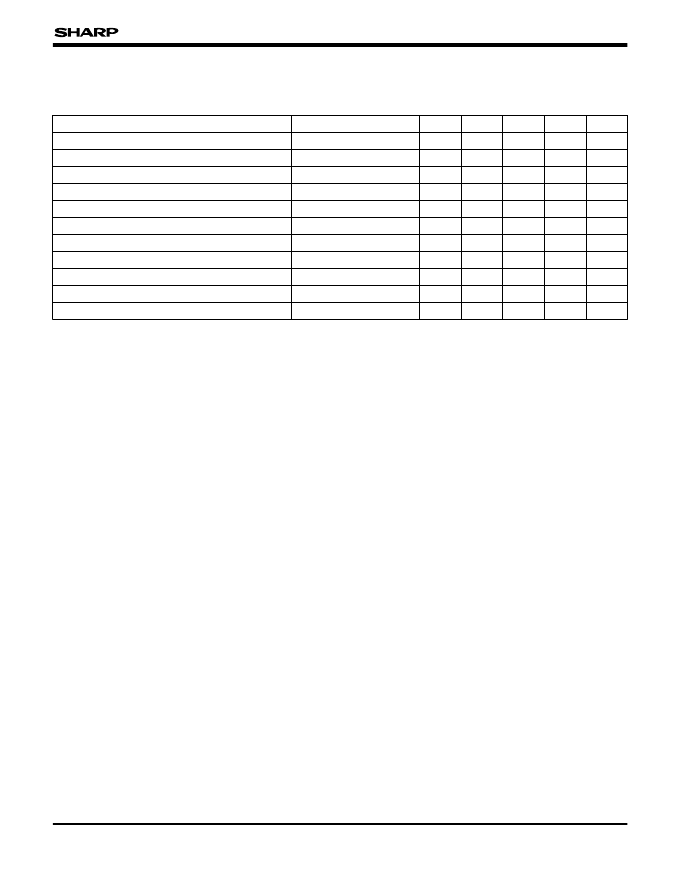
5
LZ2313H5/LZ2314HJ
CHARACTERISTICS FOR LZ2314HJ
(Drive method : Field accumulation)
(T
A
= +25 C, Operating conditions : The typical values specified in "
RECOMMENDED OPERATING CONDITIONS
".
Color temperature of light source : 3 200 K, IR cut-off filter (CM-500, 1 mmt) is used.)
PARAMETER
SYMBOL
Standard output voltage
Photo response non-uniformity
Saturation output voltage
Dark output voltage
Dark signal non-uniformity
Sensitivity
Smear ratio
Image lag
Blooming suppression ratio
Output transistor drain current
Output impedance
NOTES :
V
OFD
should be adjusted to the minimum voltage such
that ABL satisfy the specification, or to the value
displayed on the device.
1. T
A
= +60 C
2. The average output voltage under uniform illumination.
The standard exposure conditions are defined as when
Vo is 150 mV.
3. The image area is divided into 10 x 10 segments under
the standard exposure conditions. Each segment's
voltage is the average output voltage of all pixels within
the segment. PRNU is defined by (Vmax – Vmin)/Vo,
where Vmax and Vmin are the maximum and minimum
values of each segment's voltage respectively.
4. The image area is divided into 10 x 10 segments. Each
segment's voltage is the average output voltage of all
pixels within the segment. V
SAT
is the minimum
segment's voltage under 10 times exposure of the
standard exposure conditions.
5. The average output voltage under non-exposure
conditions.
6. The image area is divided into 10 x 10 segments under
non-exposure conditions. DSNU is defined by (Vdmax –
Vdmin), where Vdmax and Vdmin are the maximum and
minimum values of each segment's voltage respectively.
MIN.
TYP.
150
MAX.
UNIT
mV
%
mV
mV
mV
mV
dB
%
NOTE
2
3
4
1, 5
1, 6
7
8
9
10
V
O
PRNU
V
SAT
V
DARK
DSNU
R
SMR
AI
ABL
I
OD
R
O
10
700
0.3
0.6
800
–90
3.0
2.0
560
–76
1.0
100
4.0
350
8.0
mA
$
7. The average output voltage when a 1 000 lux light
source with a 90% reflector is imaged by a lens of F4,
f50 mm.
8. The sensor is exposed only in the central area of V/10
square with a lens at F4, where V is the vertical image
size. SMR is defined by the ratio of the output voltage
detected during the vertical blanking period to the
maximum output voltage in the V/10 square.
9. The sensor is exposed at the exposure level
corresponding to the standard conditions. AI is defined
by the ratio of the output voltage measured at the 1st
field during the non-exposure period to the standard
output voltage.
10. The sensor is exposed only in the central area of V/10
square, where V is the vertical image size. ABL is
defined by the ratio of the exposure at the standard
conditions to the exposure at a point where blooming is
observed.
相關(guān)PDF資料 |
PDF描述 |
|---|---|
| LZ2316AR | Dual-power-supply (5 V/12 V) Operation 1/3-type CCD Area Sensors with 270 k Pixels |
| LZ2323H5 | PLUG, D, FILTERED, 330PF, 62WAY; Connector type:D Sub, High-Density; Gender:Plug; Ways, No. of:62; Termination method:Solder; Material, contact:Copper Alloy; Plating, contact:Bright Tin; Series:FHTB; Material:Steel; Current RoHS Compliant: Yes |
| LZ2325A | Dual-power-supply (5 V/12 V) Operation 1/3-type CCD Area Sensors with 320 k Pixels |
| LZ2336 | Two-power supply (+5 V and +12 V) operation 1 / 3 type B/W CCD Area Sensor for EIA |
| LZ2346 | Twopower supply (+5 V and +12 V) operation CCIR 1/3 type B/W CCD Area Sensor for CCIR |
相關(guān)代理商/技術(shù)參數(shù) |
參數(shù)描述 |
|---|---|
| LZ2314J | 制造商:未知廠家 制造商全稱:未知廠家 功能描述:Area CCD Image Array |
| LZ23-15 | 制造商:ebm-papst Inc 功能描述:Metal Finger Guard |
| LZ2315A | 制造商:SHARP 制造商全稱:Sharp Electrionic Components 功能描述:Dual-power-supply (5 V/12 V) Operation 1/3-type CCD Area Sensors with 270 k Pixels |
| LZ2316AF | 制造商:Sharp Microelectronics 功能描述:1/3 CCD |
| LZ2316AJ | 制造商:未知廠家 制造商全稱:未知廠家 功能描述:AREA CCD IMAGE ARRAY |
發(fā)布緊急采購,3分鐘左右您將得到回復(fù)。