- 您現(xiàn)在的位置:買賣IC網(wǎng) > PDF目錄45001 > LV8414CS STEPPER MOTOR CONTROLLER, 0.6 A, PBGA32 PDF資料下載
參數(shù)資料
| 型號: | LV8414CS |
| 元件分類: | 運動控制電子 |
| 英文描述: | STEPPER MOTOR CONTROLLER, 0.6 A, PBGA32 |
| 封裝: | WLP-32 |
| 文件頁數(shù): | 36/36頁 |
| 文件大小: | 451K |
| 代理商: | LV8414CS |
第1頁第2頁第3頁第4頁第5頁第6頁第7頁第8頁第9頁第10頁第11頁第12頁第13頁第14頁第15頁第16頁第17頁第18頁第19頁第20頁第21頁第22頁第23頁第24頁第25頁第26頁第27頁第28頁第29頁第30頁第31頁第32頁第33頁第34頁第35頁當前第36頁
LV8414CS
No.A1868-9/36
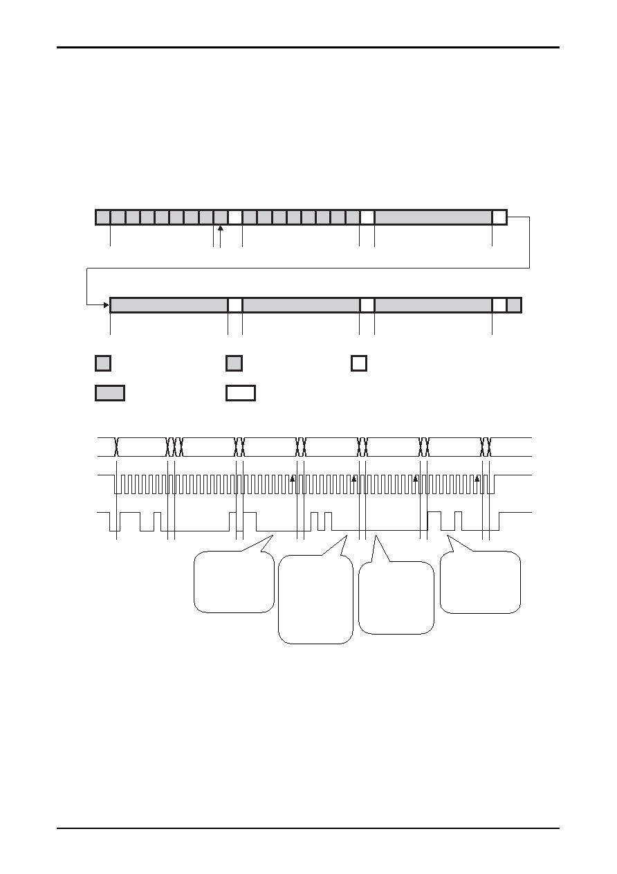
Data transfer write format
The slave address and Write command must be allocated to the first byte (8 bits) and the register address in the “Serial
data truth table” must be designated in the second byte.
For the third byte, data transfer is carried out to the address designated by the register address which is written in the
second byte. Subsequently, if data continues, the register address value is automatically incremented for the fourth and
subsequent bytes.
Thus, continuous data transfer starting at the designated address is made possible.
When the register address is set to “00000011,” the address to which the next byte is transferred wraps around to
"00000000."
(1) Data write example
(2) Actual example of continuous data transfer
Based on the “Serial data truth table” on the next page, the following settings are used for the actual example of the
continuous data transfer shown in the above figure.
(Data transfer is set at the SCL rising edge of “D0” of each data.)
1/2-channel settings:
Output ON, reset release, reverse (CCW) rotation, current reference voltage setting of 0.2V, no CLK1 frequency
division, 1-2 phase setting
3/4-channel settings:
Output ON, reset release, forward (CW) rotation, current reference voltage setting of 0.2V, no CLK2 frequency
division, 1-2 phase setting
Other settings:
400kHz chopping frequency, photo sensor OFF, MO output channels set to 1/2 channels, current reference voltage
setting of 0.2V
S
1
0
1
0
A
0
1
A
Data 1
Write data to register address
00000001
Register address set
(00000001)
Slave address
Start condition
P Stop condition
Master side transmission
Slave side transmission
A Acknowledge
R/W = 0 written
A
Data 2
A
Data 3
A
Data 4
Write data to register address
00000000
Write data to register address
00000011
Write data to register address
00000010
A
P
3/4-channel
Output on
Reset release
Forward rotation
Current reference
voltage 0.2V
1/2-channel
CLK1 frequency
division
1-2 phase setting
3/4-channel
CLK2 frequency
division
1-2 phase setting
400kHz chopping
photo sensor OFF
MO output
channels set to 1/2
channels
MO output Initial
position
1/2-channel
Output on
Reset release
Reverse rotation
Current reference
voltage 0.2V
A7 A6 A5 A4 A3 A2 A1 A0
0 0 0 000 0 1
1 1 1 001 0 0
D7 D6 D5 D4 D3 D2 D1 D0
11 0 0 0 0 0 0
D7 D6 D5 D4 D3 D2 D1 D0
0 1 0 100 0 0
D7 D6 D5 D4 D3 D2 D1 D0
0 0 0 000 0 0
D7 D6 D5 D4 D3 D2 D1 D0
11 0 0 1 0 0 0
SCL
Start
Stop
SDA
M
S
B
L
S
B
M
S
B
L
S
B
M
S
B
L
S
B
M
S
B
L
S
B
M
S
B
L
S
B
M
S
B
L
S
B
A
C
K
A
C
K
A
C
K
A
C
K
A
C
K
A
C
K
W
Slave
address
Register
address
Data
相關PDF資料 |
PDF描述 |
|---|---|
| LV8481CS | STEPPER MOTOR CONTROLLER, PBGA10 |
| LV8731V | STEPPER MOTOR CONTROLLER, PDSO44 |
| LV8743V | 0.8 A SWITCHING CONTROLLER, 440 kHz SWITCHING FREQ-MAX, PDSO44 |
| LV8743V | 0.8 A SWITCHING CONTROLLER, 440 kHz SWITCHING FREQ-MAX, PDSO44 |
| LV8746V | STEPPER MOTOR CONTROLLER, 1.2 A, PDSO44 |
相關代理商/技術參數(shù) |
參數(shù)描述 |
|---|---|
| LV8414CS_12 | 制造商:SANYO 制造商全稱:Sanyo Semicon Device 功能描述:Microstep Driver Motor Driver IC |
| LV8414CS-N-TE-L-H | 制造商:ON Semiconductor 功能描述:STEPPING MOTOR DRIVER - Tape and Reel 制造商:ON Semiconductor 功能描述:REEL / STEPPING MOTOR DRIVER |
| LV8414CS-TE-L-H | 功能描述:馬達/運動/點火控制器和驅動器 MICROSTEP MOTOR RoHS:否 制造商:STMicroelectronics 產品:Stepper Motor Controllers / Drivers 類型:2 Phase Stepper Motor Driver 工作電源電壓:8 V to 45 V 電源電流:0.5 mA 工作溫度:- 25 C to + 125 C 安裝風格:SMD/SMT 封裝 / 箱體:HTSSOP-28 封裝:Tube |
| LV8415CB | 制造商:SANYO 制造商全稱:Sanyo Semicon Device 功能描述:Blurring correction driver IC for DSC H bridge x 2ch driver |
| LV8415CB_12 | 制造商:SANYO 制造商全稱:Sanyo Semicon Device 功能描述:Blurring correction driver IC for DSC H bridge ?? 2ch driver |
發(fā)布緊急采購,3分鐘左右您將得到回復。