- 您現(xiàn)在的位置:買(mǎi)賣(mài)IC網(wǎng) > PDF目錄369872 > LUCL9313GP-D Line Interface and Line Access Circuit Full-Feature SLIC and Ringing for TR-57 Applications PDF資料下載
參數(shù)資料
| 型號(hào): | LUCL9313GP-D |
| 英文描述: | Line Interface and Line Access Circuit Full-Feature SLIC and Ringing for TR-57 Applications |
| 中文描述: | 線路接口和線路接入電路全功能SLIC和敲響訓(xùn)練班- 57應(yīng)用 |
| 文件頁(yè)數(shù): | 25/40頁(yè) |
| 文件大小: | 746K |
| 代理商: | LUCL9313GP-D |
第1頁(yè)第2頁(yè)第3頁(yè)第4頁(yè)第5頁(yè)第6頁(yè)第7頁(yè)第8頁(yè)第9頁(yè)第10頁(yè)第11頁(yè)第12頁(yè)第13頁(yè)第14頁(yè)第15頁(yè)第16頁(yè)第17頁(yè)第18頁(yè)第19頁(yè)第20頁(yè)第21頁(yè)第22頁(yè)第23頁(yè)第24頁(yè)當(dāng)前第25頁(yè)第26頁(yè)第27頁(yè)第28頁(yè)第29頁(yè)第30頁(yè)第31頁(yè)第32頁(yè)第33頁(yè)第34頁(yè)第35頁(yè)第36頁(yè)第37頁(yè)第38頁(yè)第39頁(yè)第40頁(yè)

Data Sheet
September 2001
Full-Feature SLIC and Ringing Relay for TR-57 Applications
L9313 Line Interface and Line Access Circuit
Agere Systems Inc.
25
Applications
(continued)
dc Characteristics
(continued)
Automatic Battery Switch
(continued)
The equation governing the switch point is as follows:
R
LOOP
=
–
2R
P
–
R
dc
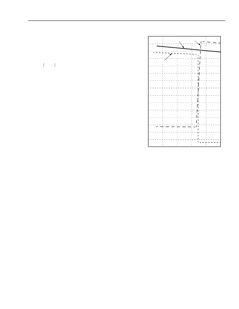
A graph showing loop and battery current versus loop
resistance with use of the battery switch is shown in
Figure 11.
The V
BAT2
voltage must be chosen properly so that the
power dissipation is minimized. When the voltage at
pin PR equals V
BAT2
+ 1 V + (50
x I
LOOP
), at least
98% of the loop current minus 2.5 mA flows into V
BAT2
and 2.5 mA + 2% of the loop current plus quiescent
current flows into V
BAT1
.
To choose V
BAT2
, add:
1. Maximum tip overhead voltage (2 V for V
OVH
= 0).
2. Maximum loop voltage (maximum loop resistance,
protection resistance, and dc feed resistance
[100
] times the maximum loop current limit).
3. 1 V for the soft switch.
Thus, for a 40 mA current limit, 640
loop, 30
pro-
tection resistors, and 3.17 dBm signal (V
OVH
= 0):
V
BAT2
=
–
(2 + 0.042 x (100 + 60 + 640) + 1) =
–
36.6 V
Then, for any loop resistance from 0
to 640
, the
worst-case V
BAT1
and V
BAT2
currents will be:
I
BAT1
= 1.39 mA + 2.5 mA + 0.02 x (42 mA
–
2.5 mA) =
4.68 mA
I
BAT2
= (0.98) x 42 mA = 38.71 mA
Total max power = 1.641 W (V
BAT
=
–
48 V)
Note that to minimize power statistically, this may not
be the best choice for V
BAT2
. Over a large number of
lines, power is minimized according to the statistical
distribution of loop resistance.
12-3470a (F)
Figure 11. L9313 Loop/Battery Current (with Battery
Switch) vs. Loop Resistance
Power Control Resistor
Device temperature rise may be controlled with use of
a single battery voltage by use of a power control resis-
tor. This technique will reduce power dissipation on the
chip, by sharing the total power not dissipated in the
loop between the L9313 and the power control resistor.
It does not, however, reduce the total power con-
sumed, as does use of the auxiliary battery. The power
control resistor is connected from the primary battery to
the V
BAT2
/PWR node of the device.
The magnitude of the power control resistor must be
low enough to ensure that sufficient power is dissipated
on the resistor to ensure the L9313 does not exceed its
thermal shutdown temperature. At the same time, the
more power that is dissipated by the power control
resistor, the higher the resistor’s power rating must be,
and thus, the more costly the resistor. The following
equations are used to optimize the choice (magnitude
and power rating) of the power control resistor.
-----------------------------------
I
LIM
0
200
0.000
0.004
0.010
R
LOOP
(
)
400
B
600
1000
800
0.016
I
LOOPdc
I
BAT1
I
BAT2
0.002
0.006
0.012
0.018
0.008
0.014
0.020
0.022
0.024
0.026
0.028
0.030
相關(guān)PDF資料 |
PDF描述 |
|---|---|
| LUCL9313GP-DT | Line Interface and Line Access Circuit Full-Feature SLIC and Ringing for TR-57 Applications |
| LUCV4914AAE | Application Specific Amplifier |
| LUCV5002AS | Voltage-Feedback Operational Amplifier |
| LUCV5006AS | Voltage-Feedback Operational Amplifier |
| LUCV5006ASI | Voltage-Feedback Operational Amplifier |
相關(guān)代理商/技術(shù)參數(shù) |
參數(shù)描述 |
|---|---|
| LUCL9313GPDT | 制造商:AGERE 功能描述:New |
| LUCL9313GP-DT | 制造商:AGERE 制造商全稱:AGERE 功能描述:Line Interface and Line Access Circuit Full-Feature SLIC and Ringing for TR-57 Applications |
| LUCL9500 | 制造商:AGERE 制造商全稱:AGERE 功能描述:High-Voltage Ringing SLIC for VolP Applications |
| LUCL9500AGF-D | 制造商:AGERE 制造商全稱:AGERE 功能描述:High-Voltage Ringing SLIC for VolP Applications |
| LUCL9500AGF-DT | 制造商:AGERE 制造商全稱:AGERE 功能描述:High-Voltage Ringing SLIC for VolP Applications |
發(fā)布緊急采購(gòu),3分鐘左右您將得到回復(fù)。