- 您現(xiàn)在的位置:買賣IC網(wǎng) > PDF目錄44998 > LTC6801IG#PBF (LINEAR TECHNOLOGY CORP) 1-CHANNEL POWER SUPPLY SUPPORT CKT, PDSO36 PDF資料下載
參數(shù)資料
| 型號(hào): | LTC6801IG#PBF |
| 廠商: | LINEAR TECHNOLOGY CORP |
| 元件分類: | 電源管理 |
| 英文描述: | 1-CHANNEL POWER SUPPLY SUPPORT CKT, PDSO36 |
| 封裝: | LEAD FREE, PLASTIC, SSOP-36 |
| 文件頁數(shù): | 23/28頁 |
| 文件大小: | 265K |
| 代理商: | LTC6801IG#PBF |
第1頁第2頁第3頁第4頁第5頁第6頁第7頁第8頁第9頁第10頁第11頁第12頁第13頁第14頁第15頁第16頁第17頁第18頁第19頁第20頁第21頁第22頁當(dāng)前第23頁第24頁第25頁第26頁第27頁第28頁
LTC6801
4
6801fb
ELECTRICAL CHARACTERISTICS The l denotes the specications which apply over the full operating
temperature range, otherwise specications are at TA = 25°C, V+ = 43.2V, V– = 0V unless otherwise noted.
SYMBOL
PARAMETER
CONDITIONS
MIN
TYP
MAX
UNITS
LTC6801 Single Ended Digital I/O Specications (SLT, SLTOK Pins)
VIH
Digital Input Voltage High
SLT Pin
l
2V
VIL
Digital Input Voltage Low
SLT Pin
l
0.5
V
VODL
Digital Output Voltage Low, Open Drain
SLT Pin, 10k to VREG
l
0.3
V
VOH
Digital Output Voltage High
SLTOK Pin, 10k to V–
l VREG– 0.3
V
VOL
Digital Output Voltage Low
SLTOK Pin, 10k to VREG
l
0.3
V
IPU-ST
Pull-Up Current
SLT Pin
l
2.5
5
10
μA
LTC6801 Differential Digital Input Specications (SIN/SIN, EIN/EIN Pins) (See Figure 1)
VIDH
Minimum Differential Input Voltage High
Differential Voltage Applied Between SIN
and SIN or EIN and EIN
l
1.7
V
VIDL
Minimum Differential Input Voltage Low
l
–1.7
V
VIL
Valid Input Voltage Low
Low Side of Differential Signal, Ref. to V–
l
0
1.2
V
VIH
Valid Input Voltage High
High Side of Differential Signal, Ref. to V–
l
2.5
6
V
VDHYS
Differential Input Hysteresis
1V
VOPEN
Open Circuit Voltage
l
2
2.5
3
V
RINCM
Input Resistance, Common Mode
l
100
150
kΩ
RINDIFF
Input Resistance, Differential
Between SIN to SIN, EIN to EIN
l
200
300
kΩ
LTC6801 Differential Digital Output Specications (SOUT/SOUT, EOUT/EOUT Pins)
VODH
Digital Output Voltage High
Output Pins Loaded With 100k to V–
l VREG – 0.4
V
VODL
Digital Output Voltage Low
Output Pins Loaded With 100k to VREG
l
0.4
V
LTC6801 Three-Level Digital Input Specications (OV0, OV1, UV0, UV1, HYST, DC, CC0 and CC1 Pins)
V3IH
Three-Level Digital Input Voltage High
l VREG – 0.3
V
V3IM
Three-Level Digital Input Voltage Mid
l VREF – 0.3
VREF + 0.3
V
V3IL
Three-Level Digital Input Voltage Low
l
0.3
V
IPU
Pull-Up Current
Pins DC, CC0, CC1, UV0 and UV1
l
0.5
1
2
μA
IPD
Pull-Down Current
Pins HYST, OV0 and OV1
l
0.5
1
2
μA
Note 1: Stresses beyond those listed under Absolute Maximum Ratings
may cause permanent damage to the device. Exposure to any Absolute
Maximum Rating condition for extended periods may affect device
reliability and lifetime.
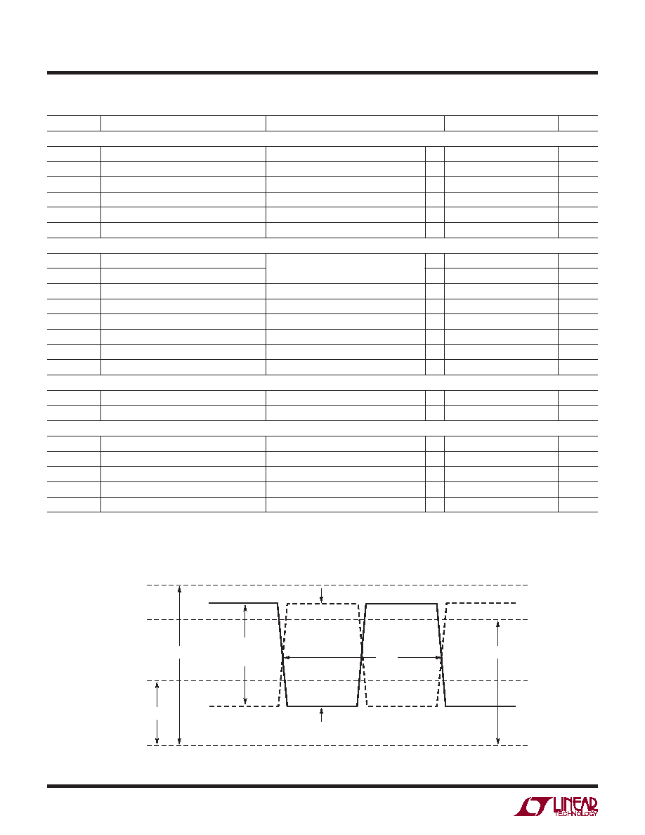
Figure 1. Differential Input Specications
6801 F01
V – = 0V
EIN
VIDH
(VALID HIGH WHEN
EIN – EIN ≥ VIDH)
MAX, VIH
TENA
MIN, VIH
MAX, VIL
VIDL
(VALID LOW WHEN EIN – EIN ≤ VIDL)
Note 2: VCELL refers to the voltage applied across the following pin
combinations: Cn to Cn – 1 for n = 2 to 12, C1 to V–.
Note 3: Guaranteed by continuous monitoring supply current
specications, not subject to test.
相關(guān)PDF資料 |
PDF描述 |
|---|---|
| LTC693IS#PBF | 1-CHANNEL POWER SUPPLY SUPPORT CKT, PDSO16 |
| LTC694CN-3.3 | 2-CHANNEL POWER SUPPLY MANAGEMENT CKT, PDIP8 |
| LTC694IN-3.3 | 2-CHANNEL POWER SUPPLY MANAGEMENT CKT, PDIP8 |
| LTC694CN8-3.3#TRPBF | 1-CHANNEL POWER SUPPLY MANAGEMENT CKT, PDIP8 |
| LTC695CN-3.3#TRPBF | 1-CHANNEL POWER SUPPLY MANAGEMENT CKT, PDIP16 |
相關(guān)代理商/技術(shù)參數(shù) |
參數(shù)描述 |
|---|---|
| LTC6801IGTRPBF | 制造商:LINER 制造商全稱:Linear Technology 功能描述:Independent Multicell Battery Stack Fault Monitor |
| LTC6802-1 | 制造商:LINER 制造商全稱:Linear Technology 功能描述:Multicell Battery Stack Monitor |
| LTC6802-1_1 | 制造商:LINER 制造商全稱:Linear Technology 功能描述:Multicell Battery Stack Monitor |
| LTC6802-2 | 制造商:LINER 制造商全稱:Linear Technology 功能描述:Multicell Battery Stack Monitor |
| LTC6802IG-1 | 制造商:LINER 制造商全稱:Linear Technology 功能描述:Multicell Battery Stack Monitor |
發(fā)布緊急采購(gòu),3分鐘左右您將得到回復(fù)。