- 您現(xiàn)在的位置:買賣IC網(wǎng) > PDF目錄44998 > LTC6604CUFF-15#TRPBF (LINEAR TECHNOLOGY CORP) SPECIALTY ANALOG CIRCUIT, PQCC34 PDF資料下載
參數(shù)資料
| 型號: | LTC6604CUFF-15#TRPBF |
| 廠商: | LINEAR TECHNOLOGY CORP |
| 元件分類: | 模擬信號調(diào)理 |
| 英文描述: | SPECIALTY ANALOG CIRCUIT, PQCC34 |
| 封裝: | 4 X 7 MM, 0.75 MM HEIGHT, LEAD FREE, PLASTIC, QFN-34 |
| 文件頁數(shù): | 4/16頁 |
| 文件大小: | 203K |
| 代理商: | LTC6604CUFF-15#TRPBF |
LT6604-15
12
660415fa
Common Mode DC Currents
In applications like Figure 1 and Figure 3 where the LT6604-15
not only provides lowpass ltering but also level shifts the
common mode voltage of the input signal, DC currents
will be generated through the DC path between input and
output terminals. Minimize these currents to decrease
power dissipation and distortion. Consider the application
in Figure 3. VMID sets the output common mode voltage of
the 1st differential amplier inside the LT6604-15 channel
(see the Block Diagram section) at 2.5V. Since the input
common mode voltage is near 0V, there will be approxi-
mately a total of 2.5V drop across the series combination
of the internal 536Ω feedback resistor and the external
133Ω input resistor. The resulting 3.7mA common mode
DC current in each input path, must be absorbed by the
sources VIN+ and VIN–. VOCM sets the common mode
output voltage of the 2nd differential amplier inside the
LT6604-15 channel, and therefore sets the common mode
output voltage of the lter. Since, in the example of Figure
3, VOCM differs from VMID by 0.5V, an additional 2.5mA
(1.25mA per side) of DC current will ow in the resistors
coupling the 1st differential amplier output stage to the
lter output. Thus, a total of 9.9mA per channel is used
to translate the common mode voltages.
A simple modication to Figure 3 will reduce the DC com-
mon mode currents by 40%. If VMID is shorted to VOCM
the common mode output voltage of both op amp stages
will be 2V and the resulting DC current will be 6mA per
channel. Of course, by AC coupling the inputs of Figure 3,
the common mode DC current can be reduced to 2.5mA
per channel.
Noise
The noise performance of the LT6604-15 channel can
be evaluated with the circuit of Figure 6. Given the low
noise output of the LT6604-15 and the 6dB attenuation
of the transformer coupling network, it will be necessary
to measure the noise oor of the spectrum analyzer and
subtract the instrument noise from the lter noise mea-
surement.
Example: With the IC removed and the 25Ω resistors
grounded, Figure 6, measure the total integrated noise
(eS) of the spectrum analyzer from 10kHz to 15MHz. With
the IC inserted, the signal source (VIN) disconnected, and
the input resistors grounded, measure the total integrated
noise out of the lter (eO).Withthesignalsourceconnected,
set the frequency to 1 MHz and adjust the amplitude until
VIN measures 100mVP-P. Measure the output amplitude,
VOUT, and compute the passband gain A = VOUT/VIN. Now
compute the input referred integrated noise (eIN) as:
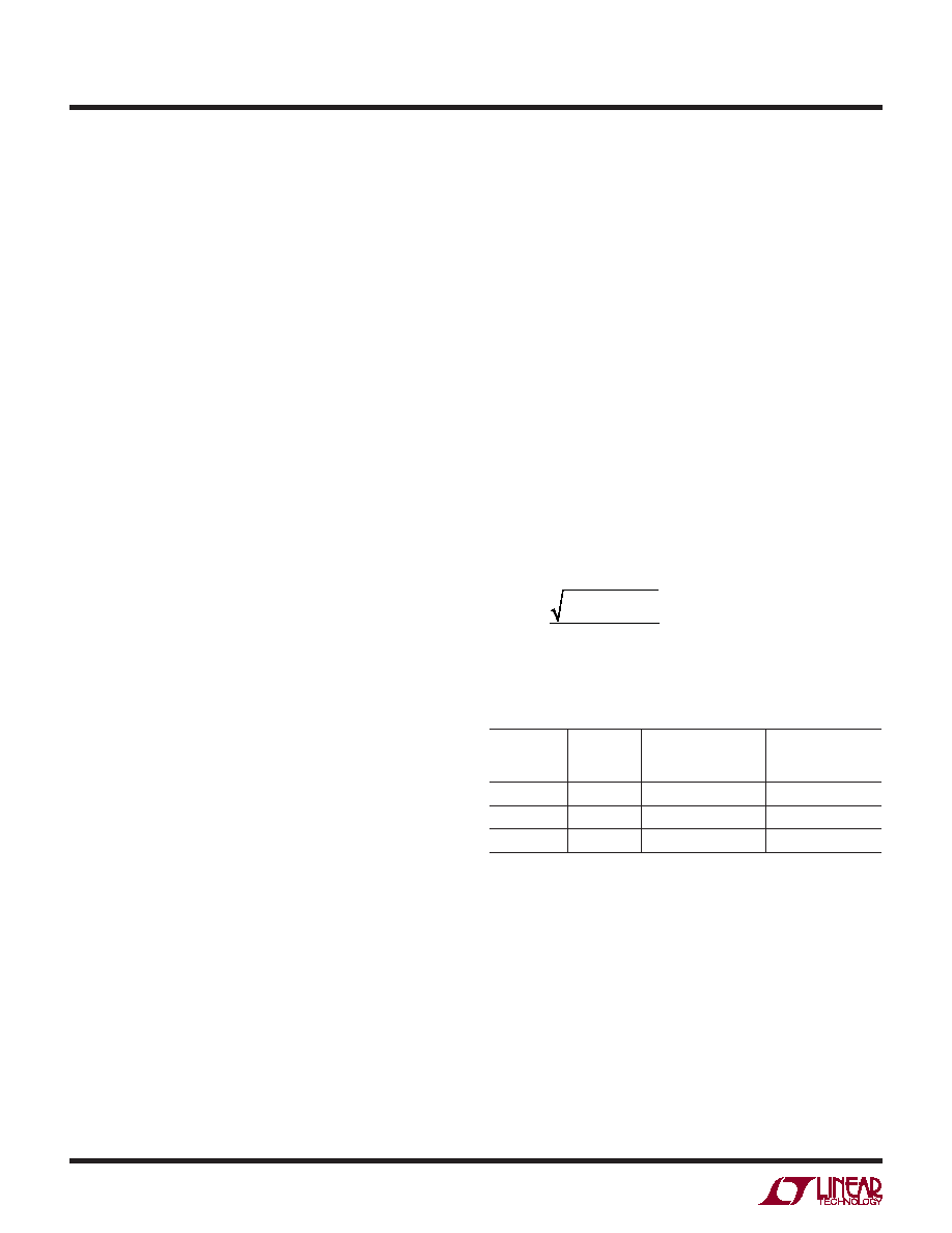
eIN =
(eO)
2 –(e
S )
2
A
Table 1 lists the typical input referred integrated noise for
various values of RIN.
Table 1. Noise Performance
PASSBAND
GAIN
RIN
INPUT REFERRED
INTEGRATED NOISE
10kHz TO 15MHz
INPUT REFERRED
INTEGRATED NOISE
10kHz TO 30MHz
4133Ω
36μVRMS
51μVRMS
2267Ω
62μVRMS
92μVRMS
1536Ω
109μVRMS
169μVRMS
APPLICATIONS INFORMATION
相關(guān)PDF資料 |
PDF描述 |
|---|---|
| LTC6652AHMS8-2.5 | 1-OUTPUT THREE TERM VOLTAGE REFERENCE, 2.5 V, PDSO8 |
| LTC6652BHMS8-2.5 | 1-OUTPUT THREE TERM VOLTAGE REFERENCE, 2.5 V, PDSO8 |
| LTC6801HG#TRPBF | 1-CHANNEL POWER SUPPLY SUPPORT CKT, PDSO36 |
| LTC6801IG#TRPBF | 1-CHANNEL POWER SUPPLY SUPPORT CKT, PDSO36 |
| LTC6801IG#PBF | 1-CHANNEL POWER SUPPLY SUPPORT CKT, PDSO36 |
相關(guān)代理商/技術(shù)參數(shù) |
參數(shù)描述 |
|---|---|
| LTC6604IUFF-10-TRPBF | 制造商:LINER 制造商全稱:Linear Technology 功能描述:Dual Very Low Noise, Differential Amplifi er and 10MHz Lowpass Filter |
| LTC6604IUFF-15-TRPBF | 制造商:LINER 制造商全稱:Linear Technology 功能描述:Dual Very Low Noise, Differential Amplifi er and 15MHz Lowpass Filter |
| LTC6605-10 | 制造商:LINER 制造商全稱:Linear Technology 功能描述:16-Bit, 20Msps Low Power ADC |
| LTC6605-14 | 制造商:LINER 制造商全稱:Linear Technology 功能描述:16-Bit, 20Msps Low Power ADC |
| LTC6605-7 | 制造商:LINER 制造商全稱:Linear Technology 功能描述:16-Bit, 20Msps Low Power Dual ADC |
發(fā)布緊急采購,3分鐘左右您將得到回復(fù)。