- 您現(xiàn)在的位置:買賣IC網(wǎng) > PDF目錄44993 > LTC3786EUD#PBF (LINEAR TECHNOLOGY CORP) SWITCHING CONTROLLER, 900 kHz SWITCHING FREQ-MAX, PQCC16 PDF資料下載
參數(shù)資料
| 型號: | LTC3786EUD#PBF |
| 廠商: | LINEAR TECHNOLOGY CORP |
| 元件分類: | 穩(wěn)壓器 |
| 英文描述: | SWITCHING CONTROLLER, 900 kHz SWITCHING FREQ-MAX, PQCC16 |
| 封裝: | 3 X 3 MM, LEAD FREE, PLASTIC, MO-220WEED-2,QFN-16 |
| 文件頁數(shù): | 10/34頁 |
| 文件大小: | 397K |
| 代理商: | LTC3786EUD#PBF |
第1頁第2頁第3頁第4頁第5頁第6頁第7頁第8頁第9頁當(dāng)前第10頁第11頁第12頁第13頁第14頁第15頁第16頁第17頁第18頁第19頁第20頁第21頁第22頁第23頁第24頁第25頁第26頁第27頁第28頁第29頁第30頁第31頁第32頁第33頁第34頁
LTC3786
18
3786fa
applicaTions inForMaTion
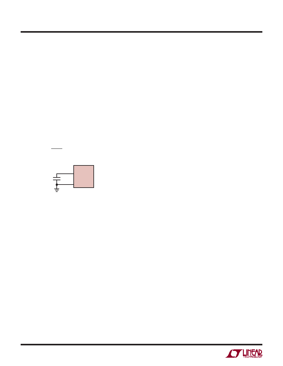
Soft-Start (SS Pin)
The start-up of the VOUT is controlled by the voltage on
the SS pin. When the voltage on the SS pin is less than
the internal 1.2V reference, the LTC3786 regulates the VFB
pin voltage to the voltage on the SS pin instead of 1.2V.
Soft-startisenabledbysimplyconnectingacapacitorfrom
the SS pin to ground, as shown in Figure 4. An internal
10A current source charges the capacitor, providing a
linear ramping voltage at the SS pin. The LTC3786 will
regulate the VFB pin (and hence, VOUT) according to the
voltage on the SS pin, allowing VOUT to rise smoothly
from VIN to its final regulated value. The total soft-start
time will be approximately:
tSS = CSS
1.2V
10A
temperature, the LTC3786 INTVCC current is limited to
less than 20mA in the QFN package from a 40V supply:
TJ = 70°C + (20mA)(40V)(68°C/W) = 125°C
In an MSOP package, the INTVCC current is limited to less
than 34mA from a 40V supply:
TJ = 70°C + (34mA)(40V)(40°C/W) = 125°C
To prevent the maximum junction temperature from being
exceeded, the input supply current must be checked while
operating in continuous conduction mode (PLLIN/MODE
= INTVCC) at maximum VBIAS.
Topside MOSFET Driver Supply (CB, DB)
External bootstrap capacitors, CB, connected to the
BOOST pin supplies the gate drive voltage for the topside
MOSFET. Capacitor CB in the Block Diagram is charged
though external diode, DB, from INTVCC when the SW pin
is low. When the topside MOSFET is to be turned on, the
driver places the CB voltage across the gate-source of the
desired MOSFET. This enhances the MOSFET and turns on
the topside switch. The switch node voltage, SW, rises to
VOUTandtheBOOSTpinfollows.WiththetopsideMOSFET
on, the boost voltage is above the output voltage: VBOOST
= VOUT + VINTVCC. The value of the boost capacitor, CB,
needs to be 100 times that of the total input capacitance
of the topside MOSFET(s). The reverse breakdown of the
external Schottky diode must be greater than VIN(MAX).
The external diode DB can be a Schottky diode or silicon
diode, but in either case it should have low leakage and fast
recovery. Pay close attention to the reverse leakage at high
temperatures where it generally increases substantially.
The topside MOSFET driver includes an internal charge
pump that delivers current to the bootstrap capacitor from
the BOOST pin. This charge current maintains the bias
voltage required to keep the top MOSFET on continuously
during dropout/overvoltage conditions. The Schottky/
silicon diode selected for the topside driver should have a
reverse leakage less than the available output current the
charge pump can supply. Curves displaying the available
charge pump current under different operating conditions
can be found in the Typical Performance Characteristics
section.
LTC3786
SS
CSS
SGND
3786 F04
Figure 4. Using the SS Pin to Program Soft-Start
INTVCC Regulator
The LTC3786 features an internal P-channel low dropout
linear regulator (LDO) that supplies power at the INTVCC
pin from the VBIAS supply pin. INTVCC powers the gate
drivers and much of the LTC3786’s internal circuitry. The
VBIAS LDO regulates INTVCC to 5.4V. It can supply at least
50mA and must be bypassed to ground with a minimum
of 4.7F ceramic capacitor. Good bypassing is needed to
supplythehightransientcurrentsrequiredbytheMOSFET
gate drivers.
High input voltage applications in which large MOSFETs
are being driven at high frequencies may cause the
maximum junction temperature rating for the LTC3786
to be exceeded. The power dissipation for the IC is equal
to VBIAS IINTVCC. The gate charge current is dependent
on operating frequency, as discussed in the Efficiency
Considerations section. The junction temperature can be
estimated by using the equations given in Note 2 of the
Electrical Characteristics. For example, at 70°C ambient
相關(guān)PDF資料 |
PDF描述 |
|---|---|
| LTC3787IGN#TRPBF | SWITCHING CONTROLLER, 585 kHz SWITCHING FREQ-MAX, PDSO28 |
| LTC3787EGN#TRPBF | SWITCHING CONTROLLER, 585 kHz SWITCHING FREQ-MAX, PDSO28 |
| LTC3787EUFD#PBF | SWITCHING CONTROLLER, 585 kHz SWITCHING FREQ-MAX, PQCC28 |
| LTC3787IGN#PBF | SWITCHING CONTROLLER, 585 kHz SWITCHING FREQ-MAX, PDSO28 |
| LTC3788EUH#TRPBF | DUAL SWITCHING CONTROLLER, 900 kHz SWITCHING FREQ-MAX, PQCC32 |
相關(guān)代理商/技術(shù)參數(shù) |
參數(shù)描述 |
|---|---|
| LTC3786IMSE#PBF | 功能描述:IC REG CTRLR BST PWM CM 16-MSOP RoHS:是 類別:集成電路 (IC) >> PMIC - 穩(wěn)壓器 - DC DC 切換控制器 系列:- 標(biāo)準(zhǔn)包裝:2,500 系列:- PWM 型:電流模式 輸出數(shù):1 頻率 - 最大:500kHz 占空比:96% 電源電壓:4 V ~ 36 V 降壓:無 升壓:是 回掃:無 反相:無 倍增器:無 除法器:無 Cuk:無 隔離:無 工作溫度:-40°C ~ 125°C 封裝/外殼:24-WQFN 裸露焊盤 包裝:帶卷 (TR) |
| LTC3786IMSE#TRPBF | 功能描述:IC REG CTRLR BST PWM CM 16-MSOP RoHS:是 類別:集成電路 (IC) >> PMIC - 穩(wěn)壓器 - DC DC 切換控制器 系列:- 標(biāo)準(zhǔn)包裝:2,500 系列:- PWM 型:電流模式 輸出數(shù):1 頻率 - 最大:500kHz 占空比:96% 電源電壓:4 V ~ 36 V 降壓:無 升壓:是 回掃:無 反相:無 倍增器:無 除法器:無 Cuk:無 隔離:無 工作溫度:-40°C ~ 125°C 封裝/外殼:24-WQFN 裸露焊盤 包裝:帶卷 (TR) |
| LTC3786IUD#PBF | 功能描述:IC REG CTRLR BST PWM CM 16-QFN RoHS:是 類別:集成電路 (IC) >> PMIC - 穩(wěn)壓器 - DC DC 切換控制器 系列:- 標(biāo)準(zhǔn)包裝:2,500 系列:- PWM 型:電流模式 輸出數(shù):1 頻率 - 最大:500kHz 占空比:96% 電源電壓:4 V ~ 36 V 降壓:無 升壓:是 回掃:無 反相:無 倍增器:無 除法器:無 Cuk:無 隔離:無 工作溫度:-40°C ~ 125°C 封裝/外殼:24-WQFN 裸露焊盤 包裝:帶卷 (TR) |
| LTC3786IUD#TRPBF | 功能描述:IC REG CTRLR BST PWM CM 16-QFN RoHS:是 類別:集成電路 (IC) >> PMIC - 穩(wěn)壓器 - DC DC 切換控制器 系列:- 標(biāo)準(zhǔn)包裝:2,500 系列:- PWM 型:電流模式 輸出數(shù):1 頻率 - 最大:500kHz 占空比:96% 電源電壓:4 V ~ 36 V 降壓:無 升壓:是 回掃:無 反相:無 倍增器:無 除法器:無 Cuk:無 隔離:無 工作溫度:-40°C ~ 125°C 封裝/外殼:24-WQFN 裸露焊盤 包裝:帶卷 (TR) |
| LTC3787EGN#PBF | 功能描述:IC REG CTRLR BST PWM CM 28-SSOP RoHS:是 類別:集成電路 (IC) >> PMIC - 穩(wěn)壓器 - DC DC 切換控制器 系列:PolyPhase® 特色產(chǎn)品:LM3753/54 Scalable 2-Phase Synchronous Buck Controllers 標(biāo)準(zhǔn)包裝:1 系列:PowerWise® PWM 型:電壓模式 輸出數(shù):1 頻率 - 最大:1MHz 占空比:81% 電源電壓:4.5 V ~ 18 V 降壓:是 升壓:無 回掃:無 反相:無 倍增器:無 除法器:無 Cuk:無 隔離:無 工作溫度:-5°C ~ 125°C 封裝/外殼:32-WFQFN 裸露焊盤 包裝:Digi-Reel® 產(chǎn)品目錄頁面:1303 (CN2011-ZH PDF) 其它名稱:LM3754SQDKR |
發(fā)布緊急采購,3分鐘左右您將得到回復(fù)。