- 您現(xiàn)在的位置:買賣IC網(wǎng) > PDF目錄296330 > LTC2206IUK-14#TRPBF (LINEAR TECHNOLOGY CORP) 16-Bit, 80Msps ADC; Package: QFN; No of Pins: 48; Temperature Range: -40°C to +85°C PDF資料下載
參數(shù)資料
| 型號(hào): | LTC2206IUK-14#TRPBF |
| 廠商: | LINEAR TECHNOLOGY CORP |
| 元件分類: | ADC |
| 英文描述: | 16-Bit, 80Msps ADC; Package: QFN; No of Pins: 48; Temperature Range: -40°C to +85°C |
| 中文描述: | 1-CH 14-BIT PROPRIETARY METHOD ADC, PARALLEL ACCESS, PQCC48 |
| 封裝: | 7 X 7 MM, LEAD FREE, PLASTIC, MO-220WKKD-2, QFN-48 |
| 文件頁(yè)數(shù): | 7/32頁(yè) |
| 文件大小: | 1237K |
| 代理商: | LTC2206IUK-14#TRPBF |
第1頁(yè)第2頁(yè)第3頁(yè)第4頁(yè)第5頁(yè)第6頁(yè)當(dāng)前第7頁(yè)第8頁(yè)第9頁(yè)第10頁(yè)第11頁(yè)第12頁(yè)第13頁(yè)第14頁(yè)第15頁(yè)第16頁(yè)第17頁(yè)第18頁(yè)第19頁(yè)第20頁(yè)第21頁(yè)第22頁(yè)第23頁(yè)第24頁(yè)第25頁(yè)第26頁(yè)第27頁(yè)第28頁(yè)第29頁(yè)第30頁(yè)第31頁(yè)第32頁(yè)
LTC2207-14/LTC2206-14
15
220714614fc
PIN FUNCTIONS
OF (Pin 43): Over/Under Flow Digital Output. OF is high
when an over or under ow has occurred.
OE (Pin 44): Output Enable Pin. Low enables the digital
output drivers. High puts digital outputs in Hi-Z state.
MODE (Pin 45): Output Format and Clock Duty Cycle
Stabilizer Selection Pin. Connecting MODE to 0V selects
offset binary output format and disables the clock duty
cycle stabilizer. Connecting MODE to 1/3VDD selects offset
binary output format and enables the clock duty cycle sta-
bilizer. Connecting MODE to 2/3VDDselects2’scomplement
output format and enables the clock duty cycle stabilizer.
Connecting MODE to VDD selects 2’s complement output
format and disables the clock duty cycle stabilizer.
RAND (Pin 46): Digital Output Randomization Selection
Pin. RAND low results in normal operation. RAND high
selects D1-D13 to be EXCLUSIVE-ORed with D0 (the
LSB). The output can be decoded by again applying an
XOR operation between the LSB and all other bits. This
mode of operation reduces the effects of digital output
interference.
PGA(Pin47):ProgrammableGainAmplierControlPin.Low
selects a front-end gain of 1, input range of 2.25VP-P. High
selects a front-end gain of 1.5, input range of 1.5VP-P.
GND (Exposed Pad, Pin 49): ADC Power Ground. The ex-
posed pad on the bottom of the package must be soldered
to ground.
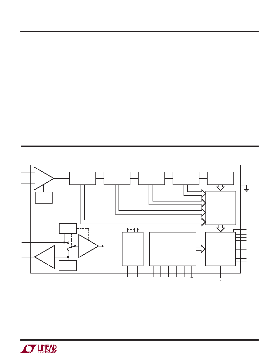
DITH
OE
MODE
PGA RAND
SHDN
ADC CLOCKS
DIFFERENTIAL
INPUT
LOW JITTER
CLOCK
DRIVER
DITHER
SIGNAL
GENERATOR
FIRST PIPELINED
ADC STAGE
FIFTH PIPELINED
ADC STAGE
FOURTH PIPELINED
ADC STAGE
SECOND PIPELINED
ADC STAGE
ENC+
ENC–
CORRECTION LOGIC
AND
SHIFT REGISTER
OGND
CLKOUT+
CLKOUT–
OF
D13
D12
OVDD
D1
D0
2207614 F01
INPUT
S/H
AIN
–
AIN
+
THIRD PIPELINED
ADC STAGE
OUTPUT
DRIVERS
CONTROL
LOGIC
VDD
GND
PGA
SENSE
VCM
BUFFER
ADC
REFERENCE
VOLTAGE
REFERENCE
RANGE
SELECT
Figure 1. Functional Block Diagram
BLOCK DIAGRAM
相關(guān)PDF資料 |
PDF描述 |
|---|---|
| LTC2207CUK-14#PBF | 16-Bit, 105Msps ADC; Package: QFN; No of Pins: 48; Temperature Range: 0°C to +70°C |
| LTC2207CUK-14#TRPBF | 16-Bit, 105Msps ADC; Package: QFN; No of Pins: 48; Temperature Range: 0°C to +70°C |
| LTC2207IUK-14#PBF | 16-Bit, 105Msps ADC; Package: QFN; No of Pins: 48; Temperature Range: -40°C to +85°C |
| LTC2207IUK-14#TRPBF | 16-Bit, 105Msps ADC; Package: QFN; No of Pins: 48; Temperature Range: -40°C to +85°C |
| LTC2206CUK#PBF | 16-Bit, 80Msps ADC; Package: QFN; No of Pins: 48; Temperature Range: 0°C to +70°C |
相關(guān)代理商/技術(shù)參數(shù) |
參數(shù)描述 |
|---|---|
| LTC2206UK | 制造商:LINER 制造商全稱:Linear Technology 功能描述:16-Bit, 105Msps/80Msps ADCs |
| LTC2206UK-14 | 制造商:LINER 制造商全稱:Linear Technology 功能描述:14-Bit, 105Msps/80Msps ADCs |
| LTC2207 | 制造商:LINER 制造商全稱:Linear Technology 功能描述:16-Bit, 20Msps Low Power ADC |
| LTC2207-14 | 制造商:LINER 制造商全稱:Linear Technology 功能描述:14-Bit, 105Msps/80Msps ADCs |
| LTC2207CUK | 制造商:Linear Technology 功能描述:ADC Single Pipelined 105Msps 16-bit Parallel 48-Pin QFN EP |
發(fā)布緊急采購(gòu),3分鐘左右您將得到回復(fù)。