- 您現(xiàn)在的位置:買賣IC網(wǎng) > PDF目錄44987 > LT4180MPGN#TRPBF (LINEAR TECHNOLOGY CORP) POWER SUPPLY SUPPORT CKT, PDSO24 PDF資料下載
參數(shù)資料
| 型號: | LT4180MPGN#TRPBF |
| 廠商: | LINEAR TECHNOLOGY CORP |
| 元件分類: | 電源管理 |
| 英文描述: | POWER SUPPLY SUPPORT CKT, PDSO24 |
| 封裝: | 0.150 INCH, LEAD FREE, PLASTIC, SSOP-24 |
| 文件頁數(shù): | 17/18頁 |
| 文件大?。?/td> | 278K |
| 代理商: | LT4180MPGN#TRPBF |
LT4180
8
4180fa
INTRODUCTION
The LT4180 is designed to interface with a variety of power
supplies and regulators having either an external feedback
or control pin. In Figure 4, the regulator error amplier
(which is a gm amplier) is disabled by tying its inverting
input to ground. This converts the error amplier into a
constant-current source which is then controlled by the
drain pin of the LT4180. This is the preferred method of
interfacing because it eliminates the regulator error ampli-
er from the control loop which simplies compensation
and provides best control loop response.
APPLICATIONS INFORMATION
Figure 4. Nonisolated Regulator Interface
For proper operation, increasing control voltage should
correspond to increasing regulator output. For example,
in the case of a current mode switching power supply, the
control pin ITH should produce higher peak currents as
the ITH pin voltage is made more positive.
Figure 5. Isolated Power Supply Interface
Figure 6. Cascoded DRAIN Pin for Isolated Supplies
DRAIN
4180 F04
LT4180
ITH OR
VC
REGULATOR
+
–
DRAIN
4180 F05
LT4180
VC
INTVCC
REGULATOR
OPTO-COUPLER
+
–
DRAIN
4180 F06
INTVCC
LT4180
TO VC > 5V
COMP
from degrading contacts. Making the capacitor larger can
minimize the voltage ripple at the load due to a combination
of load regulation and the dither frequency of the LT4180.
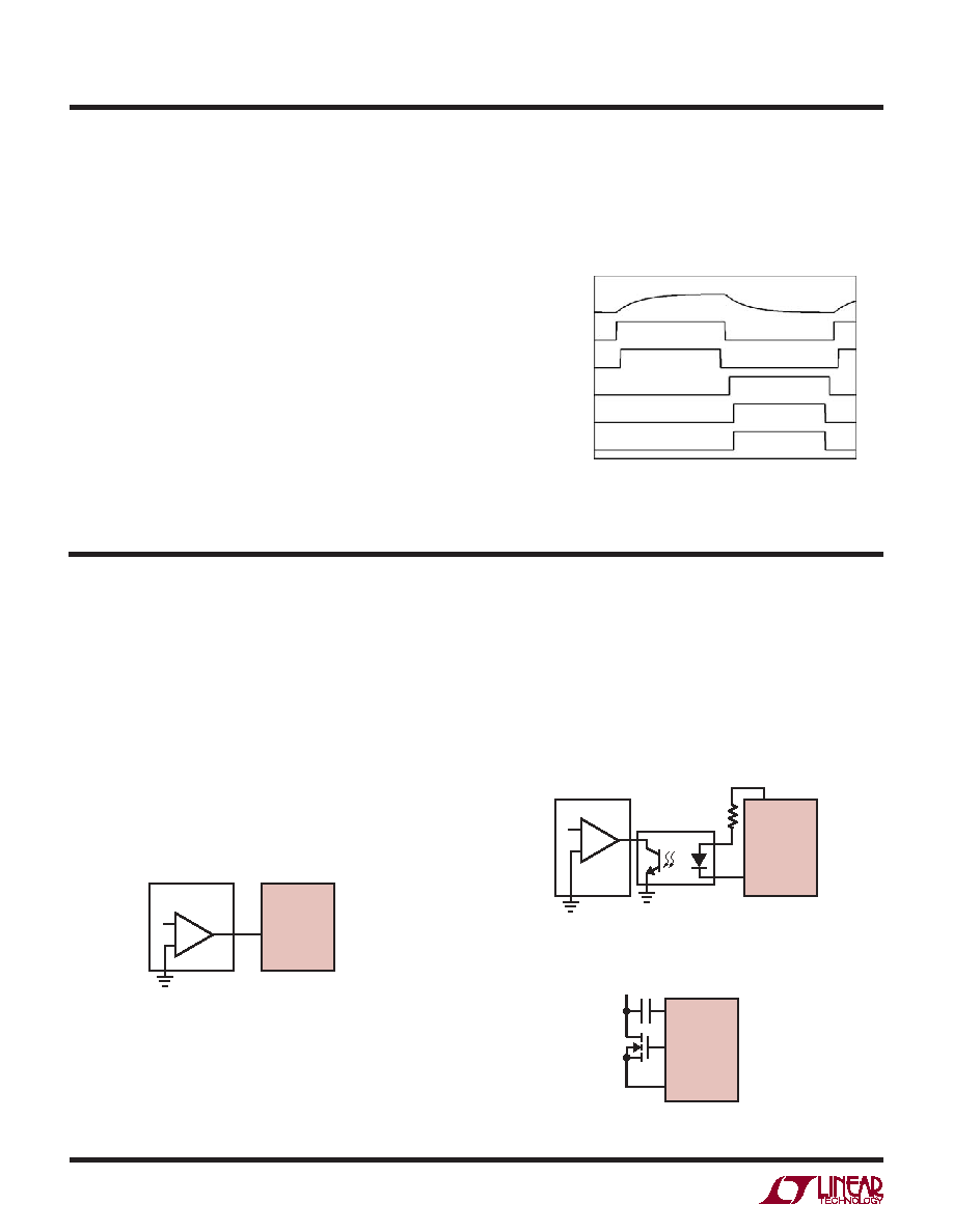
Figure 3 shows the timing diagram for Virtual Remote
Sense. A new cycle begins when the power supply and
Virtual Remote Sense close the loop around VOUT (regulate
VOUT = H). Both VOUT and IOUT slew and settle to a new
value, and these values are stored in the Virtual Remote
Sense (track VOUT high = L and track IOUT = L). The VOUT
feedback loop is opened and a new feedback loop is set
up commanding the power supply to deliver 90% of the
previously measured current (0.9IOUT).VOUTdropstoanew
value as the power supply reaches a new steady state, and
this information is also stored in the Virtual Remote Sense.
At this point, the change in output voltage (ΔVOUT) for a
Figure 3. Simplied Timing Diagram, Virtual Remote Sense
VOUT
TRACK ΔVOUT
REGULATE VOUT
TRACK VOUT HIGH
TRACK IOUT
REGULATE IOUT LOW
TRACK VOUT LOW
4180 F03
Isolated power supplies and regulators may also be used
by adding an opto-coupler (Figure 5). LT4180 output volt-
age INTVCC supplies power to the opto-coupler LED. In
situations where the control pin VC of the regulator may
exceed 5V, a cascode may be added to keep the DRAIN
pin of the LT4180 below 5V (Figure 6). Use a low VT
MOSFET for the cascode transistor.
–10% change in output current has been measured and
is stored in the Virtual Remote Sense. This voltage is used
during the next Virtual Remote Sense cycle to compensate
for voltage drops due to wiring resistance.
OPERATION
相關PDF資料 |
PDF描述 |
|---|---|
| LT4250HCN8#TRPBF | 1-CHANNEL POWER SUPPLY SUPPORT CKT, PDIP8 |
| LT4356CS-3 | SPECIALTY ANALOG CIRCUIT, PDSO16 |
| LT4356IMS-3 | SPECIALTY ANALOG CIRCUIT, PDSO10 |
| LT4356HMS-3#PBF | SPECIALTY ANALOG CIRCUIT, PDSO10 |
| LT4356IS-3 | SPECIALTY ANALOG CIRCUIT, PDSO16 |
相關代理商/技術參數(shù) |
參數(shù)描述 |
|---|---|
| LT41EC | 制造商:LAUREL ELECTRONICS 功能描述:LT Series transmitter with dual solid state relays, isolated 4-20 mA and RS232/R |
| LT41EF | 制造商:LAUREL ELECTRONICS 功能描述:LT Series transmitter with dual solid state relays, isolated 4-20 mA and RS232/R |
| LT41JF | 制造商:LAUREL ELECTRONICS 功能描述:LT Series transmitter with dual solid state relays, isolated 4-20 mA and RS232/R |
| LT41KC | 制造商:LAUREL ELECTRONICS 功能描述:LT Series transmitter with dual solid state relays, isolated 4-20 mA and RS232/R |
| LT41KF | 制造商:LAUREL ELECTRONICS 功能描述:LT Series transmitter with dual solid state relays, isolated 4-20 mA and RS232/R |
發(fā)布緊急采購,3分鐘左右您將得到回復。