- 您現(xiàn)在的位置:買賣IC網(wǎng) > PDF目錄44968 > LSN-1.3/10-D12BJ 1-OUTPUT DC-DC REG PWR SUPPLY MODULE PDF資料下載
參數(shù)資料
| 型號(hào): | LSN-1.3/10-D12BJ |
| 元件分類: | 電源模塊 |
| 英文描述: | 1-OUTPUT DC-DC REG PWR SUPPLY MODULE |
| 封裝: | SIP-11/9 |
| 文件頁數(shù): | 5/12頁 |
| 文件大小: | 753K |
| 代理商: | LSN-1.3/10-D12BJ |
LSN-10A D12 Series
N O N - I S O L A T E D , 1 0 - 5 0 W S I P D C / D C C O N V E R T E R S
LSN-1/10-D12
1
10
45
65
±0.1%
±0.25%
12
10.8-13.2
39/1.02
83%
86%
B5/B5x, P59
LSN-1.1/10-D12
1.1
10
45
60
±0.1%
±0.25%
12
10.8-13.2
45/1.1
85%
88%
87.5%
B5/B5x, P59
LSN-1.2/10-D12
1.2
10
45
60
±0.1%
±0.25%
12
10.8-13.2
45/1.19
85%
88%
87.5%
B5/B5x, P59
LSN-1.3/10-D12
1.3
10
45
60
±0.1%
±0.25%
12
10.8-13.2
45/1.3
85%
88%
87.5%
B5/B5x, P59
LSN-1.5/10-D12
1.5
10
30
45
±0.1%
±0.25%
12
10.8-13.2
54/1.47
86%
89%
88%
B5/B5x, P59
LSN-1.8/10-D12
1.8
10
30
45
±0.1%
±0.25%
12
10.8-13.2
53/1.75
87%
90.5%
89.5%
B5/B5x, P59
LSN-2/10-D12
2
10
30
45
±0.1%
±0.25%
12
10.8-13.2
59/1.9
88.5%
91%
90%
B5/B5x, P59
LSN-2.5/10-D12
2.5
10
35
50
±0.1%
±0.25%
12
10.8-13.2
60/2.3
90.5%
92.5%
92%
B5/B5x, P59
LSN-3.3/10-D12
3.3
10
40
55
±0.1%
±0.25%
12
10.8-13.2
69/3
92.5%
94%
93.5%
B5/B5x, P59
LSN-5/10-D12
5
10
50
75
±0.1%
±0.25%
12
10.8-13.2
75/4.5
94%
96%
95.5%
B5/B5x, P59
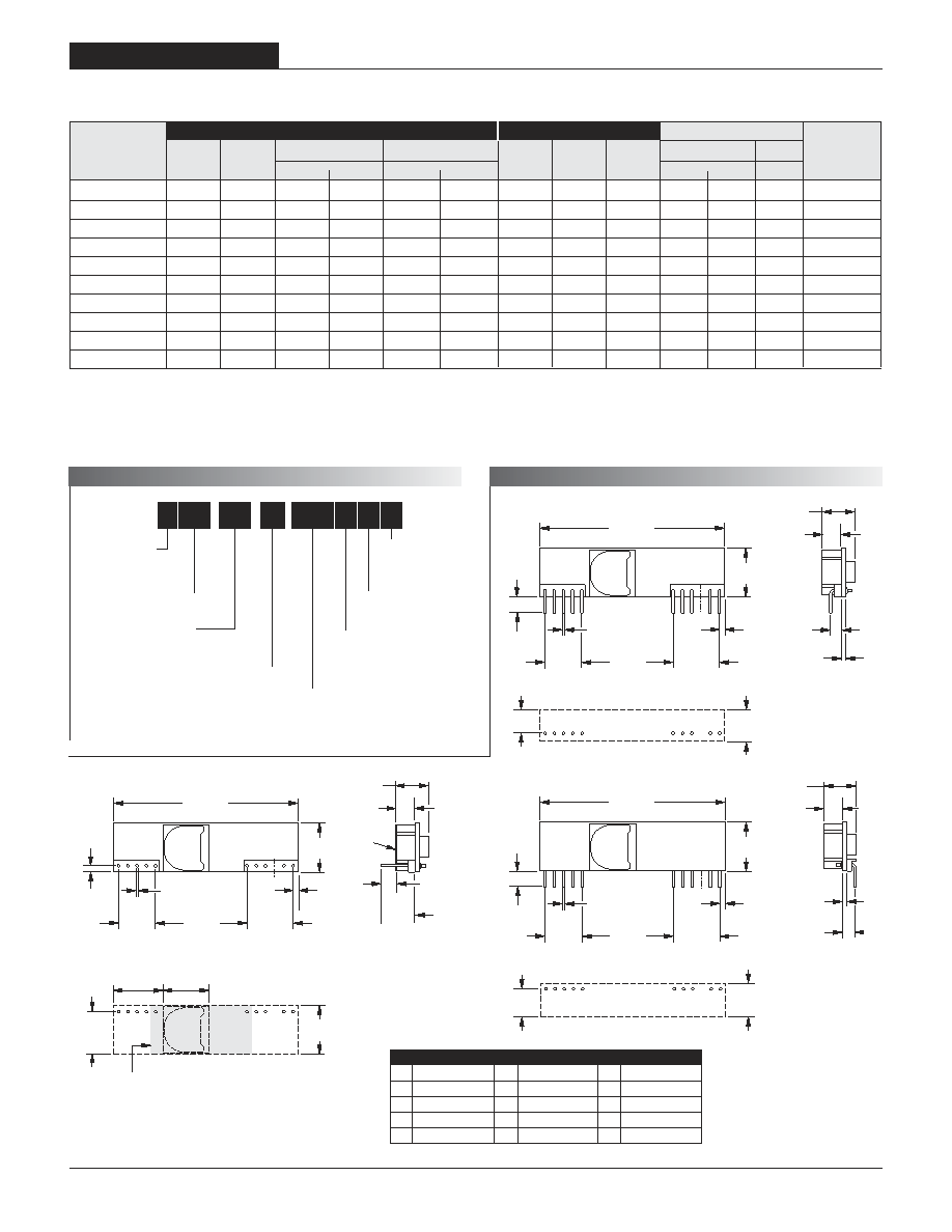
1 2 3 4 5
7
6
8 9 10 11
2.00
(50.80)
0.030 ±0.001 DIA.
(0.762 ±0.025)
0.55
(13.97)
0.34
(8.64)
0.20
(5.08)
0.110
(2.79)
0.046
(1.17)
0.05
(1.27)
0.400
(10.16)
4 EQ. SP. @
0.100 (2.54)
0.500
(12.70)
5 EQ. SP. @
0.100 (2.54)
1.000
(25.40)
0.17
(4.32)
LAYOUT PATTERN
TOP VIEW
0.34
(8.64)
0.25
(6.35)
2
Typical at TA = +25°C under nominal line voltage and full-load conditions, unless otherwise
noted. All models are tested and specied with external 22F tantalum input and output
capacitors. These capacitors are necessary to accommodate our test equipment and may
not be required to achieve specied performance in your applications. See I/O Filtering and
Noise Reduction.
M E C H A N I C A L
S P E C I F I C A T I O N S
Case B5
Vertical Mounting
(Standard)
Ripple/Noise (R/N) is tested/specied over a 20MHz bandwidth and may be
reduced with external ltering. See I/O Filtering and Noise Reduction for details.
These devices have no minimum-load requirements and will regulate under no-load conditions.
Regulation specications describe the output-voltage deviation as the line voltage or load is
varied from its nominal/midpoint value to either extreme.
Nominal line voltage, no-load/full-load conditions.
P A R T
N U M B E R
S T R U C T U R E
* Pin 3 (+Sense) removed
for "B" sufx models.
0.35
(8.89)
0.21
(5.33)
0.16
(4.06)
0.360
(9.14)
1 2 3 4 5
7
6
8 9
ISOLATING
PAD
10 11
2.00
(50.80)
0.030 ±0.001 DIA.
(0.762 ±0.025)
0.55
(13.97)
0.05
(1.27)
0.05
(1.27)
0.55
(13.97)
0.50
(12.7)
0.400
(10.16)
0.56
(14.22)
0.53
(13.46)
4 EQ. SP. @
0.100 (2.54)
0.500
(12.70)
5 EQ. SP. @
0.100 (2.54)
1.000
(25.40)
LAYOUT PATTERN
TOP VIEW
RECOMMENDED
COPPER PAD
ON PCB (0.55 SQ. IN.)
Case B5A
Horizontal Mounting
Performance Specications and Ordering Guide
Package
VOUT
IOUT
VIN Nom.
Range
IIN
(Case,
Model
(Volts)
(Amps)
Typ.
Max.
Line
Load
(Volts)
(mA/A)
Min.
Typ.
Pinout)
Output
Input
R/N (mVp-p)
Regulation (Max.)
Efciency
Full Load
Load
LAYOUT PATTERN
TOP VIEW
0.36
(9.14)
0.20
(5.08)
0.106
(2.69)
0.046
(1.17)
0.36
(9.14)
0.306
(7.8)
1 2 3 4 5
7
6
8 9 10 11
2.00
(50.80)
0.030 ±0.001 DIA.
(0.762 ±0.025)
0.55
(13.97)
0.05
(1.27)
0.400
(10.16)
4 EQ. SP. @
0.100 (2.54)
0.500
(12.70)
5 EQ. SP. @
0.100 (2.54)
1.000
(25.40)
0.17
(4.32)
Case B5B
Reverse Pin
Vertical Mounting
(Tyco-compatible)
See page 12 for Part Number
Structure and ordering details.
Pin
Function P59*
Pin
Function P59* Pin
Function P59*
1
+Output
5
Common
9
No Pin
2
+Output
6
Common
10
VOUT Trim
3
+Sense *
7
+Input
11
On/Off Control
4
+Output
8
+Input
I/O Connections
Maximum Rated Output
Current in Amps
Non-Isolated SIP
Output
Conguration:
L = Unipolar
Low Voltage
Nominal Output Voltage:
1, 1.1, 1.2, 1.3, 1.5, 1.8, 2, 2.5, 3.3
or 5 Volts
Input Voltage Range:
D12 = 10.8 to 13.2 Volts
(12V nominal)
L SN
10
-
/
D12 B
-
1.8
B Sufx:
No Remote Sense
(Pin 3 removed)
H
H Sufx:
Horizontal Mount
J
J Sufx:
Reversed Pin
Vertical Mount
相關(guān)PDF資料 |
PDF描述 |
|---|---|
| LSN-1/10-D12H | 1-OUTPUT 10 W DC-DC REG PWR SUPPLY MODULE |
| LSN-2.5/10-D12BJ | 1-OUTPUT DC-DC REG PWR SUPPLY MODULE |
| LSN-1.2/10-D12J | 1-OUTPUT DC-DC REG PWR SUPPLY MODULE |
| LSN-2/10-D12BH | 1-OUTPUT DC-DC REG PWR SUPPLY MODULE |
| LSN-2/10-D12 | 1-OUTPUT DC-DC REG PWR SUPPLY MODULE |
相關(guān)代理商/技術(shù)參數(shù) |
參數(shù)描述 |
|---|---|
| LSN1510D12J | 制造商:Datel 功能描述: |
| LSN1510D5 | 制造商:Datel 功能描述: |
| LSN16A-D12 | 制造商:MURATA 制造商全稱:Murata Manufacturing Co., Ltd. 功能描述:Single Output, Non-Isolated, 12VIN, 0.75-5VOUT 16 Amp in DC/DCs SIP Packages |
| LSN16A-W3 | 制造商:MURATA 制造商全稱:Murata Manufacturing Co., Ltd. 功能描述:Non-Isolated, 3-5.5VIN, 0.75-3.3VOUT 16 Amp DC/DC Converters |
| LSN1810D5J | 制造商:Datel 功能描述: |
發(fā)布緊急采購,3分鐘左右您將得到回復(fù)。