- 您現(xiàn)在的位置:買(mǎi)賣(mài)IC網(wǎng) > PDF目錄44953 > LS5320-9PD5B1 (POWER-ONE INC) 2-OUTPUT 100 W AC-DC PWR FACTOR CORR MODULE PDF資料下載
參數(shù)資料
| 型號(hào): | LS5320-9PD5B1 |
| 廠商: | POWER-ONE INC |
| 元件分類(lèi): | 電源模塊 |
| 英文描述: | 2-OUTPUT 100 W AC-DC PWR FACTOR CORR MODULE |
| 封裝: | METAL, CASE S02, MODULE |
| 文件頁(yè)數(shù): | 16/27頁(yè) |
| 文件大小: | 599K |
| 代理商: | LS5320-9PD5B1 |
第1頁(yè)第2頁(yè)第3頁(yè)第4頁(yè)第5頁(yè)第6頁(yè)第7頁(yè)第8頁(yè)第9頁(yè)第10頁(yè)第11頁(yè)第12頁(yè)第13頁(yè)第14頁(yè)第15頁(yè)當(dāng)前第16頁(yè)第17頁(yè)第18頁(yè)第19頁(yè)第20頁(yè)第21頁(yè)第22頁(yè)第23頁(yè)第24頁(yè)第25頁(yè)第26頁(yè)第27頁(yè)
Cassette Style
100 Watt AC-DC Converters
S Series PFC
Edition 01/01.2001
23/27
Table 19: D-output logic signals
Version of D
Ui < Ut resp. Uo < Ut
Ui > Ut + Uh resp. Uo > Ut
Conguration
D1, D2, D3, D4, D0
low
high
JFET
D5, D6, D7, D8, D9, DD
high
low
NPN
D Undervoltage Monitor
The input and/or output undervoltage monitoring circuit op-
erates independently of the built-in input undervoltage lock-
out circuit. A logic "low" (JFET output) or "high" signal (NPN
output) is generated at pin 20 as soon as one of the moni-
tored voltages drops below the preselected threshold level
Ut. The return for this signal is Vo1–. The D output recovers
when the monitored voltage(s) exceed(s)
Ut + Uh. The
Table 18: Undervoltage monitoring functions
Output type
Monitoring
Minimum adjustment range
Typical hysteresis
Uho [% of Ut]
JFET
NPN
U i
Uo1
of threshold level
U t
for
U t min...U t max
Uti
Uto
Uho
D1
D5
no
yes
-
3.5...40 V 1
2.5...0.6
D2
D6
yes
no
355V DC 4
--
D3
D7
yes
355V DC 4
(0.95...0.985
Uo1) 2
"0"
D4
D8
no
yes
-
(0.95...0.985
Uo1) 2
"0"
D0
D9
no
yes
-
3.5...40 V 3
2.5...0.6
yes
355V DC 4
3.5...40 V 3
2.5...0.6
DD
yes
355V DC 4
3.5...40 V 1
2.5...0.6
1 Threshold level adjustable by potentiometer
2 Fixed value. Tracking if Uo1 adjusted via R-input, option P or sense lines.
3 The threshold level permanently adjusted according to customer specication
±2% at 25°C. Any value within the specied range is
basically possible but causes a special type designation in addition to the standard option designations (D0/D9)!
4 Option D monitors the boost regulator output voltage. The trigger level is adjusted in the factory to 355 V DC.
threshold level
Uti is adjusted in the factory. The threshold
level
Uto is either adjusted by a potentiometer, accessible
through a hole in the front cover, or factory adjusted to a
xed value specied by the customer.
Option D exists in various versions D0...DD as shown in the
following table.
Vo1+
Vo1–
D
UD
ID
Rp
Input
11007
Vo1+
Vo1–
D
UD
ID
Rp
Input
11006
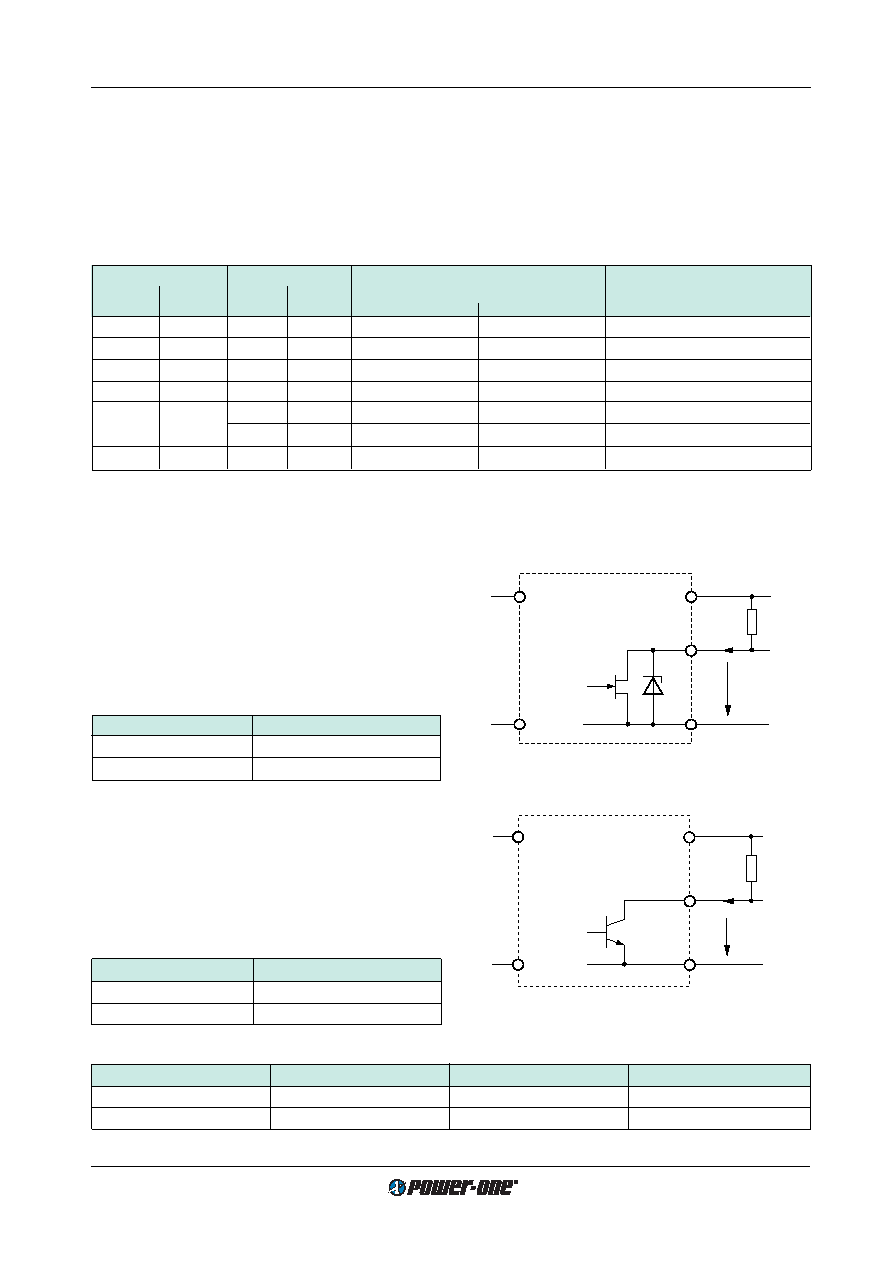
Fig. 36
Option D0...D4: JFET output, ID ≤ 2.5 mA
NPN output (D5...DD):
Connector pin D is internally connected via the collector-
emitter path of a NPN transistor to the negative potential of
output 1.
UD
< 0.4 V (logic low) corresponds to a monitored
voltage level (
Ui and/or Uo1)
> U
t + Uh. The current ID
through the open collector should not exceed 20 mA. The
NPN output is not protected against external overvoltages.
UD should not exceed 40 V.
Ui, Uo1 status
D output,
UD
Ui or Uo1 < Ut
high, H,
ID ≤ 25 A at UD = 40 V
Ui and Uo1 > Ut + Uh
low, L,
UD ≤ 0.4 V at ID = 20 mA
JFET output (D0…D4):
Connector pin D is internally connected via the drain-
source path of a JFET (self-conducting type) to the nega-
tive potential of output 1.
UD
≤ 0.4 V (logic low) corresponds
to a monitored voltage level (
Ui and/or Uo1)
<U
t. The cur-
rent
ID through the JFET should not exceed 2.5 mA. The
JFET is protected by a 0.5 W Zener diode of 8.2 V against
external overvoltages.
Ui, Uo1 status
D output,
UD
Ui or Uo1 < Ut
low, L,
UD ≤ 0.4 V at ID = 2.5 mA
Ui and Uo1 > Ut + Uh
high, H,
ID ≤ 25 A at UD = 5.25 V
Fig. 37
Option D5...DD: NPN output, Uo1
≤ 40 V, I
D
≤ 20 mA
相關(guān)PDF資料 |
PDF描述 |
|---|---|
| LS5540-7ERTB2 | 2-OUTPUT 100 W AC-DC PWR FACTOR CORR MODULE |
| LS5540-7PD0TB2 | 2-OUTPUT 100 W AC-DC PWR FACTOR CORR MODULE |
| LS5540-7PD6B2 | 2-OUTPUT 100 W AC-DC PWR FACTOR CORR MODULE |
| LS5540-9ERD0TB1 | 2-OUTPUT 100 W AC-DC PWR FACTOR CORR MODULE |
| LS5660-7EPD3TB2 | 2-OUTPUT 100 W AC-DC PWR FACTOR CORR MODULE |
相關(guān)代理商/技術(shù)參數(shù) |
參數(shù)描述 |
|---|---|
| LS5-33 | 功能描述:打印機(jī) LS5 Lam Contin Tape Polyester RoHS:否 制造商:Seiko Instruments 產(chǎn)品:Printer 電源電壓: 每行點(diǎn)數(shù):9 x 320 打印速度:52.5 cps, 80 cps 紙張寬度:112 mm |
| LS5-34 | 功能描述:打印機(jī) LS5, Laminated Continuous Tape, Polyeste RoHS:否 制造商:Seiko Instruments 產(chǎn)品:Printer 電源電壓: 每行點(diǎn)數(shù):9 x 320 打印速度:52.5 cps, 80 cps 紙張寬度:112 mm |
| LS5-35 | 功能描述:打印機(jī) LS5, Laminated Continuous Tape, Polyeste RoHS:否 制造商:Seiko Instruments 產(chǎn)品:Printer 電源電壓: 每行點(diǎn)數(shù):9 x 320 打印速度:52.5 cps, 80 cps 紙張寬度:112 mm |
| LS5-35C | 制造商:Panduit Corp 功能描述: |
| LS5360 | 制造商:INFINEON 制造商全稱(chēng):Infineon Technologies AG 功能描述:T1 (5mm) LED LAMP |
發(fā)布緊急采購(gòu),3分鐘左右您將得到回復(fù)。