- 您現(xiàn)在的位置:買賣IC網(wǎng) > PDF目錄384606 > LP3971 (National Semiconductor Corporation) POWER MANAGEMENT UNIT FOR ADVANCED APPLICATION PROCESSORS PDF資料下載
參數(shù)資料
| 型號(hào): | LP3971 |
| 廠商: | National Semiconductor Corporation |
| 英文描述: | POWER MANAGEMENT UNIT FOR ADVANCED APPLICATION PROCESSORS |
| 中文描述: | 電源管理單元提供高級(jí)應(yīng)用處理器 |
| 文件頁(yè)數(shù): | 35/42頁(yè) |
| 文件大小: | 1350K |
| 代理商: | LP3971 |
第1頁(yè)第2頁(yè)第3頁(yè)第4頁(yè)第5頁(yè)第6頁(yè)第7頁(yè)第8頁(yè)第9頁(yè)第10頁(yè)第11頁(yè)第12頁(yè)第13頁(yè)第14頁(yè)第15頁(yè)第16頁(yè)第17頁(yè)第18頁(yè)第19頁(yè)第20頁(yè)第21頁(yè)第22頁(yè)第23頁(yè)第24頁(yè)第25頁(yè)第26頁(yè)第27頁(yè)第28頁(yè)第29頁(yè)第30頁(yè)第31頁(yè)第32頁(yè)第33頁(yè)第34頁(yè)當(dāng)前第35頁(yè)第36頁(yè)第37頁(yè)第38頁(yè)第39頁(yè)第40頁(yè)第41頁(yè)第42頁(yè)
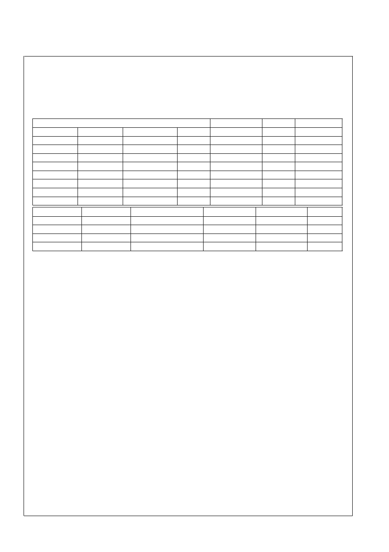
LP3971 Controls
(Continued)
GENERAL PURPOSE I/O FUNCTIONALITY (GPIO1 AND
GPIO2)
LP3971 has 2 general purpose I/Os for system control. I
2
C
compatible interface will be used for setting any of the pins to
LP3971 GPIO Control Table
input, output or hi-Z mode. Inputs value can be read via
serial interface (GPI1,2 bits). The pin 29 functionality needs
to
be
set
to
GPIO
by
serial
nEXTCHGEN.
interface
register
bit
Controls
Port Function
GPIO1
Input = 0
Input = 1
X
X
HiZ
Input (dig)-
>
Output = 0
Output= 1
Reg.
gpin 1
0
0
0
batmonchg
Function
Enabled
Not Enabled
GPIO1
<
1
>
X
X
1
X
0
1
0
1
GPIO1
<
0
>
X
X
0
X
0
0
1
1
nextchgen_sel
1
1
1
X
0
0
0
0
bucen
0
o
X
1
X
X
X
X
Enabled
0
Input
0
0
GPIO2
<
1
>
0
1
0
1
GPIO2
<
0
>
0
0
1
1
Factory fm disabled
GPIO_tstiob
1
1
1
1
GPIO2
HiZ
Input (dig)-
>
Output = 0
Output = 1
gpin2
0
Input
0
0
The LP3971 Back Up Charger can be enabled/disabled by
two separate mechanisms. They are; 1) A dedicated control
register bit named BUCEN (Register 0B Bit 2) and 2) GPIO1
input Pin 29, when configured for charger control.
Description of this operation is as follows:
In the default state, the BUCEN bit is not asserted, and
GPIO1 is configured as charger control. High level ap-
plied to GPIO1 will disable the back up charger, Low level
applied to GPIO1 will enable the back up charger. There
is an internal pull up that will disable the back up charger
if GPIO1 is “open”.
If BUCEN bit is asserted with GPIO1 configured for
charger control, the back up charger will always be en-
abled, and GPIO1 input will have no effect.
Configuration of GPIO1 charger function is via control
register bit named BBCS (Register 0E Bit 7). When this
bit is asserted (Default state), GPIO1 is charger control.
When this bit is de-asserted, charger enable is deter-
mined only by the state of control register bit BUCEN.
One additional feature of the charger enable is when the
main battery voltage Vin (Pin 6) is less than the back up
battery voltage Vin BUBATT (Pin 15), The charger will
automatically disable regardless of the input received
from BUCEN or GPIO1.
REGULATED VOLTAGES OK
All the power domains have own register bit (x_OK) that
processor can read via serial interface to be sure that en-
abled powers are OK (regulating). Note that these read only
bits are only valid when regulators are settled (avoid reading
these bits during voltage change or power up).
L
www.national.com
35
相關(guān)PDF資料 |
PDF描述 |
|---|---|
| LP3971SQ-A514 | POWER MANAGEMENT UNIT FOR ADVANCED APPLICATION PROCESSORS |
| LP3971SQ-B410 | POWER MANAGEMENT UNIT FOR ADVANCED APPLICATION PROCESSORS |
| LP3971SQX-A514 | POWER MANAGEMENT UNIT FOR ADVANCED APPLICATION PROCESSORS |
| LP3971SQX-B410 | POWER MANAGEMENT UNIT FOR ADVANCED APPLICATION PROCESSORS |
| LP3994 | 50mA CMOS Voltage Regulator with Enable Control |
相關(guān)代理商/技術(shù)參數(shù) |
參數(shù)描述 |
|---|---|
| LP3971SQ-2G16/NOPB | 功能描述:PMIC 解決方案 RoHS:否 制造商:Texas Instruments 安裝風(fēng)格:SMD/SMT 封裝 / 箱體:QFN-24 封裝:Reel |
| LP3971SQ-7848/NOPB | 功能描述:PMIC 解決方案 RoHS:否 制造商:Texas Instruments 安裝風(fēng)格:SMD/SMT 封裝 / 箱體:QFN-24 封裝:Reel |
| LP3971SQ-8858/NOPB | 功能描述:PMIC 解決方案 RoHS:否 制造商:Texas Instruments 安裝風(fēng)格:SMD/SMT 封裝 / 箱體:QFN-24 封裝:Reel |
| LP3971SQ-A514 | 制造商:NSC 制造商全稱:National Semiconductor 功能描述:POWER MANAGEMENT UNIT FOR ADVANCED APPLICATION PROCESSORS |
| LP3971SQ-B410 | 功能描述:PMIC 解決方案 RoHS:否 制造商:Texas Instruments 安裝風(fēng)格:SMD/SMT 封裝 / 箱體:QFN-24 封裝:Reel |
發(fā)布緊急采購(gòu),3分鐘左右您將得到回復(fù)。