- 您現(xiàn)在的位置:買賣IC網(wǎng) > PDF目錄384605 > LP3952RLX (NATIONAL SEMICONDUCTOR CORP) 6-Channel Color LED Driver with Audio Synchronization PDF資料下載
參數(shù)資料
| 型號: | LP3952RLX |
| 廠商: | NATIONAL SEMICONDUCTOR CORP |
| 元件分類: | 顯示驅(qū)動器 |
| 英文描述: | 6-Channel Color LED Driver with Audio Synchronization |
| 中文描述: | LED DISPLAY DRIVER, PBGA36 |
| 封裝: | 3 X 3 MM, 0.65 MM HEIGHT, 0.50 MM PITCH, MICRO, SMD-36 |
| 文件頁數(shù): | 5/44頁 |
| 文件大小: | 1621K |
| 代理商: | LP3952RLX |
第1頁第2頁第3頁第4頁當(dāng)前第5頁第6頁第7頁第8頁第9頁第10頁第11頁第12頁第13頁第14頁第15頁第16頁第17頁第18頁第19頁第20頁第21頁第22頁第23頁第24頁第25頁第26頁第27頁第28頁第29頁第30頁第31頁第32頁第33頁第34頁第35頁第36頁第37頁第38頁第39頁第40頁第41頁第42頁第43頁第44頁
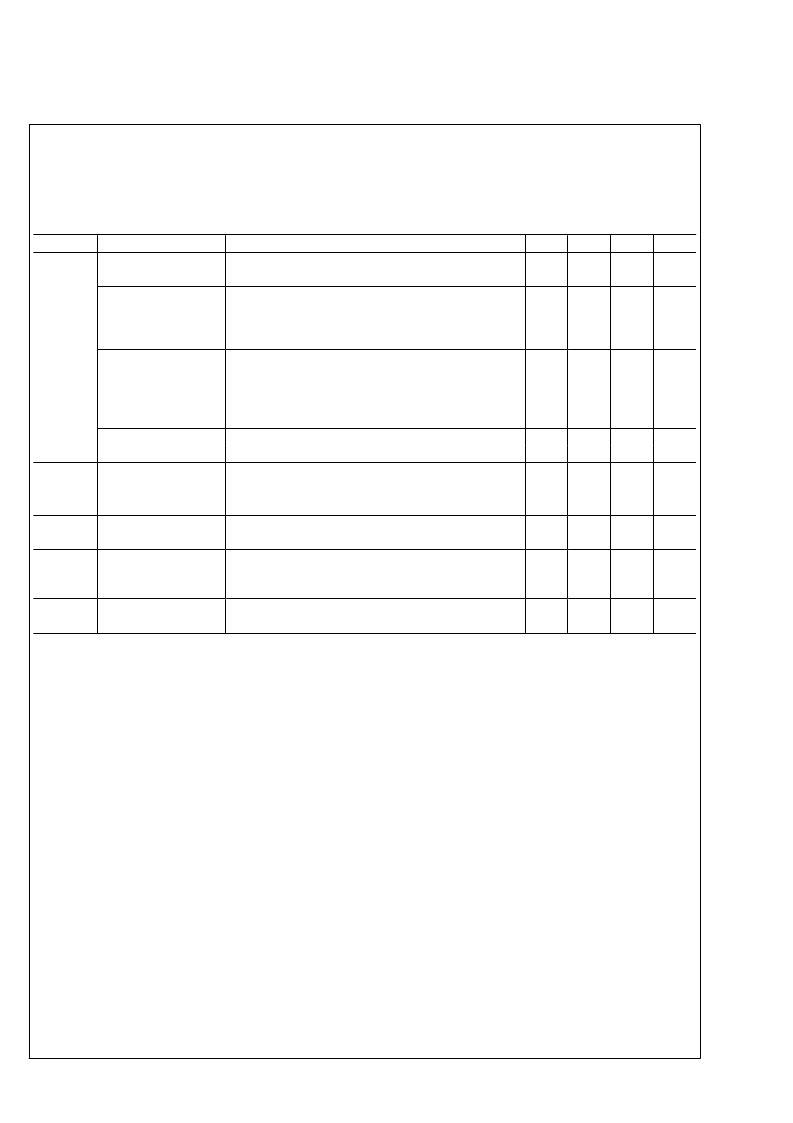
Electrical Characteristics
(Notes 2, 10)
Limits in standard typeface are for T
J
= 25°C. Limits in
boldface
type apply over the operating ambient temperature range (-30°C
< T
A
< +85°C). Unless otherwise noted, specifications apply to the LP3952 Block Diagram with: V
DD1
= V
DD2
= 3.6V, V
DDIO
= 2.8V,
C
VDD
= C
VDDIO
= 100 nF, C
OUT
= C
IN
= 10 μ
F, C
VDDA
= 1 μ
F, C
REF
= 100 nF, L
1
= 4.7 μ
H, R
RGB
= 5.6 k
Ω
and R
RT
= 82 k
Ω (
Note
11).
Symbol
Parameter
Condition
I
VDD
Standby supply current
(V
DD1
+ V
DD2
)
SCL=H, SDA = H
No-boost supply current
(V
DD1
+ V
DD2
)
EN_BOOST(bit) = L
SCL = H, SDA = H
Audio sync and LEDs OFF
No-load supply current
(V
DD1
+ V
DD2
)
EN_BOOST (bit) = H
SCL = H, SDA = H
Audio sync and LEDs OFF
Autoload OFF
RGB drivers
(V
DD1
+ V
DD2
)
SW mode
I
VDD
Audio synchronization
(V
DD1
+ V
DD2
)
V
DD1,2
= 2.8V
V
DD1,2
= 3.6V
I
VDDIO
V
DDIO
Standby Supply
current
SCL = H, SDA = H
I
EXT_LDO
External LDO output
current
(V
DD1
, V
DD2
, V
DDA
)
V
DDA
Output voltage of internal
LDO for analog parts
Min
Typ
1
Max
8
Units
μ
A
NSTBY (bit) = L, NRST (pin) = H
NSTBY (bit) = H,
450
μ
A
NSTBY (bit) = H,
1
mA
CC mode at R1, G1, B1 and R2, G2, B2 set to 15 mA
150
150
390
700
μ
A
Audio sync ON
μ
A
NSTBY (bit)=L
1
μ
A
7V tolerant application only
I
BOOST
= 300 mA
6.5
mA
(Note 12)
2.72
-3
2.80
2.88
+3
V
%
Note 1:
Absolute Maximum Ratings indicate limits beyond which damage to the component may occur. Operating Ratings are conditions under which operation
of the device is guaranteed. Operating Ratings do not imply guaranteed performance limits. For guaranteed performance limits and associated test conditions,
see the Electrical Characteristics tables.
Note 2:
All voltages are with respect to the potential at the GND pins.
Note 3:
Battery/Charger voltage should be above 6V no more than 10% of the operational lifetime.
Note 4:
Voltage tolerance of LP3952 above 6.0V relies on fact that V
and V
(2.8V) are available (ON) at all conditions. If V
DD1
and V
DD2
are not available
(ON) at all conditions, National Semiconductor does not guarantee any parameters or reliability for this device.
Note 5:
Internal thermal shutdown circuitry protects the device from permanent damage. Thermal shutdown engages at T
J
=160°C (typ.) and disengages at
T
J
=140°C (typ.).
Note 6:
For detailed soldering specifications and information, please refer to National Semiconductor Application Note AN1412 : Micro SMDxt Wafer Level Chip
Scale Package
Note 7:
The Human body model is a 100 pF capacitor discharged through a 1.5 k
resistor into each pin.
Note 8:
In applications where high power dissipation and/or poor package thermal resistance is present, the maximum ambient temperature may have to be
derated. Maximum ambient temperature (T
A-MAX
) is dependent on the maximum operating junction temperature (T
= 125°C), the maximum power
dissipation of the device in the application (P
), and the junction-to ambient thermal resistance of the part/package in the application (
θ
JA
), as given by the
following equation: T
A-MAX
= T
J-MAX-OP
– (θ
JA
× P
D-MAX
).
Note 9:
Junction-to-ambient thermal resistance is highly application and board-layout dependent. In applications where high maximum power dissipation exists,
special care must be paid to thermal dissipation issues in board design.
Note 10:
Min and Max limits are guaranteed by design, test, or statistical analysis. Typical numbers are not guaranteed, but do represent the most likely norm.
Note 11:
Low-ESR Surface-Mount Ceramic Capacitors (MLCCs) used in setting electrical characteristics.
Note 12:
V
DDA
output is not recommended for external use.
5
www.national.com
L
相關(guān)PDF資料 |
PDF描述 |
|---|---|
| LP3952RL | 6-Channel Color LED Driver with Audio Synchronization |
| LP39542 | Zener Diode; Application: Low noise; Pd (mW): 250; Vz (V): 4.3 to 4.7; Condition Iz at Vz (mA): 0.5; C (pF) max: -; Condition VR at C (V):   ESD (kV) min: -; Package: LLD |
| LP39542RL | Zener Diode; Application: Low noise; Pd (mW): 250; Vz (V): 4.6 to 5.0; Condition Iz at Vz (mA): 0.5; C (pF) max: -; Condition VR at C (V):   ESD (kV) min: -; Package: LLD |
| LP39542RLX | Zener Diode; Application: Low noise; Pd (mW): 250; Vz (V): 4.9 to 5.3; Condition Iz at Vz (mA): 0.5; C (pF) max: -; Condition VR at C (V):   ESD (kV) min: -; Package: LLD |
| LP39542TL | Advanced Lighting Management Unit |
相關(guān)代理商/技術(shù)參數(shù) |
參數(shù)描述 |
|---|---|
| LP3952RLX/NOPB | 功能描述:LED照明驅(qū)動器 RoHS:否 制造商:STMicroelectronics 輸入電壓:11.5 V to 23 V 工作頻率: 最大電源電流:1.7 mA 輸出電流: 最大工作溫度: 安裝風(fēng)格:SMD/SMT 封裝 / 箱體:SO-16N |
| LP3954 | 制造商:NSC 制造商全稱:National Semiconductor 功能描述:Advanced Lighting Management Unit |
| LP39542 | 制造商:NSC 制造商全稱:National Semiconductor 功能描述:Advanced Lighting Management Unit |
| LP39542RL | 制造商:Texas Instruments 功能描述:IC, LIGHTING MGNT UNIT, SMD |
| LP39542RL/NOPB | 功能描述:LED照明驅(qū)動器 RoHS:否 制造商:STMicroelectronics 輸入電壓:11.5 V to 23 V 工作頻率: 最大電源電流:1.7 mA 輸出電流: 最大工作溫度: 安裝風(fēng)格:SMD/SMT 封裝 / 箱體:SO-16N |
發(fā)布緊急采購,3分鐘左右您將得到回復(fù)。