- 您現(xiàn)在的位置:買賣IC網(wǎng) > PDF目錄384603 > LMV793MAX (NATIONAL SEMICONDUCTOR CORP) 88 MHz, Low Noise, 1.8V CMOS Input, Decompensated Operational Amplifiers PDF資料下載
參數(shù)資料
| 型號: | LMV793MAX |
| 廠商: | NATIONAL SEMICONDUCTOR CORP |
| 元件分類: | 運動控制電子 |
| 英文描述: | 88 MHz, Low Noise, 1.8V CMOS Input, Decompensated Operational Amplifiers |
| 中文描述: | OP-AMP, 1650 uV OFFSET-MAX, 88 MHz BAND WIDTH, PDSO8 |
| 封裝: | SOIC-8 |
| 文件頁數(shù): | 14/22頁 |
| 文件大?。?/td> | 543K |
| 代理商: | LMV793MAX |
The circuit gain for
Figure 4
at low frequencies is R
/R
, but
F, the feedback factor is not equal to the circuit gain. The
feedback factor is derived from feedback theory and is the
same for both inverting and non-inverting configurations. Yes,
the feedback factor at low frequencies is equal to the gain for
the non-inverting configuration.
(5)
From this formula, we can see that
1/F's zero is located at a lower frequency compared with
1/F's pole.
1/F's value at low frequency is 1 + R
F
/R
IN
.
This method creates one additional pole and one
additional zero.
This pole-zero pair will serve two purposes:
—
To raise the 1/F value at higher frequencies prior to its
intercept with A, the open loop gain curve, in order to
meet the G
= 10 requirement. For the LMV793/
LMV794 some overcompensation will be necessary for
good stability.
—
To achieve the previous purpose above with no
additional loop phase delay.
Please note the constraint 1/F
≥
G
needs to be satisfied
only in the vicinity where the open loop gain A and 1/F inter-
sect; 1/F can be shaped elsewhere as needed. The 1/F pole
must occur before the intersection with the open loop gain A.
In order to have adequate phase margin, it is desirable to fol-
low these two rules:
Rule 1
1/F and the open loop gain A should intersect at the
frequency where there is a minimum of 45° of phase
margin. When over-compensation is required the in-
tersection point of A and 1/F is set at a frequency
where the phase margin is above 45°, therefore in-
creasing the stability of the circuit.
Rule 2
1/F’s pole should be set at least one decade below
the intersection with the open loop gain A in order to
take advantage of the full 90° of phase lead brought
by 1/F’s pole which is F’s zero. This ensures that the
effect of the zero is fully neutralized when the 1/F and
A plots intersect each other.
Calculating Lead-Lag Compensation for LMV793/
LMV794
Figure 5
is the same plot as
Figure 1
, but the A
and phase
curves have been redrawn as smooth lines to more readily
show the concepts covered, and to clearly show the key pa-
rameters used in the calculations for lead-lag compensation.
20216348
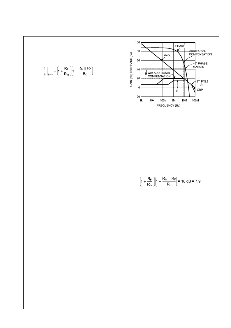
FIGURE 5. LMV793/LMV794 Simplified Bode Plot
To obtain stable operation with gains under 10 V/V the open
loop gain margin must be reduced at high frequencies to
where there is a 45° phase margin when the gain margin of
the circuit with the external compensation is 0 dB. The pole
and zero in F, the feedback factor, control the gain margin at
the higher frequencies. The distance between F and A
is
the gain margin; therefore, the unity gain point (0 dB) is where
F crosses the A
VOL
curve.
For the example being used R
= R
for a gain of 1. There-
fore F = 6 dB at low frequencies. At the higher frequencies
the minimum value for F is 18 dB for 45° phase margin. From
Equation 5
we have the following relationship:
Now set R
F
= R
= R. With these values and solving for R
C
we have R
= R/5.9. Note that the value of C does not affect
the ratio between the resistors. Once the value of the resistors
are set, then the position of the pole in F must be set. A
2 k
resistor is used for R
F
and R
IN
in this design. Therefore
the value for R
C
is set at 330
, the closest standard value for
2 k
/5.9.
Rewriting
Equation 2
to solve for the minimum capacitor value
gives the following equation:
C = 1/(2
π
f
p
R
C
)
The feedback factor curve, F, intersects the A
curve at
about 12 MHz. Therefore the pole of F should not be any
larger than 1.2 MHz. Using this value and R
= 330
the min-
imum value for C is 390 pF.
Figure 6
shows that there is too
much overshoot, but the part is stable. Increasing C to 2.2 nF
did not improve the ringing, as shown in
Figure 7
.
www.national.com
14
L
相關(guān)PDF資料 |
PDF描述 |
|---|---|
| LMV793MF | 88 MHz, Low Noise, 1.8V CMOS Input, Decompensated Operational Amplifiers |
| LMV793MFX | 88 MHz, Low Noise, 1.8V CMOS Input, Decompensated Operational Amplifiers |
| LMV794 | 88 MHz, Low Noise, 1.8V CMOS Input, Decompensated Operational Amplifiers |
| LMV794MA | 88 MHz, Low Noise, 1.8V CMOS Input, Decompensated Operational Amplifiers |
| LMV794MAX | 88 MHz, Low Noise, 1.8V CMOS Input, Decompensated Operational Amplifiers |
相關(guān)代理商/技術(shù)參數(shù) |
參數(shù)描述 |
|---|---|
| LMV793MAX/NOPB | 功能描述:運算放大器 - 運放 RoHS:否 制造商:STMicroelectronics 通道數(shù)量:4 共模抑制比(最小值):63 dB 輸入補償電壓:1 mV 輸入偏流(最大值):10 pA 工作電源電壓:2.7 V to 5.5 V 安裝風格:SMD/SMT 封裝 / 箱體:QFN-16 轉(zhuǎn)換速度:0.89 V/us 關(guān)閉:No 輸出電流:55 mA 最大工作溫度:+ 125 C 封裝:Reel |
| LMV793MF | 制造商:Texas Instruments 功能描述:OP AMP, DECOM, 1.8V, 88MHZ, POWERWISE 制造商:Texas Instruments 功能描述:OP AMP, DECOM, 1.8V, 88MHZ, POWERWISE; Op Amp Type:Low Noise; No. of Amplifiers:1; Slew Rate:40V/s; Supply Voltage Range:1.8V to 5.5V; Amplifier Case Style:SOT-23; No. of Pins:5; Bandwidth:88MHz; Operating Temperature Min:-40C; ;RoHS Compliant: Yes |
| LMV793MF/NOPB | 功能描述:運算放大器 - 運放 RoHS:否 制造商:STMicroelectronics 通道數(shù)量:4 共模抑制比(最小值):63 dB 輸入補償電壓:1 mV 輸入偏流(最大值):10 pA 工作電源電壓:2.7 V to 5.5 V 安裝風格:SMD/SMT 封裝 / 箱體:QFN-16 轉(zhuǎn)換速度:0.89 V/us 關(guān)閉:No 輸出電流:55 mA 最大工作溫度:+ 125 C 封裝:Reel |
| LMV793MFX | 制造商:NSC 制造商全稱:National Semiconductor 功能描述:88 MHz, Low Noise, 1.8V CMOS Input, Decompensated Operational Amplifiers |
| LMV793MFX/NOPB | 功能描述:運算放大器 - 運放 RoHS:否 制造商:STMicroelectronics 通道數(shù)量:4 共模抑制比(最小值):63 dB 輸入補償電壓:1 mV 輸入偏流(最大值):10 pA 工作電源電壓:2.7 V to 5.5 V 安裝風格:SMD/SMT 封裝 / 箱體:QFN-16 轉(zhuǎn)換速度:0.89 V/us 關(guān)閉:No 輸出電流:55 mA 最大工作溫度:+ 125 C 封裝:Reel |
發(fā)布緊急采購,3分鐘左右您將得到回復。