- 您現(xiàn)在的位置:買(mǎi)賣(mài)IC網(wǎng) > PDF目錄384603 > LMD18200T (NATIONAL SEMICONDUCTOR CORP) 3A, 55V H-Bridge PDF資料下載
參數(shù)資料
| 型號(hào): | LMD18200T |
| 廠商: | NATIONAL SEMICONDUCTOR CORP |
| 元件分類(lèi): | 外設(shè)及接口 |
| 英文描述: | 3A, 55V H-Bridge |
| 中文描述: | 6 A HB BASED PRPHL DRVR WITH PWM, ZFM11 |
| 封裝: | TO-220, 11 PIN |
| 文件頁(yè)數(shù): | 7/13頁(yè) |
| 文件大小: | 439K |
| 代理商: | LMD18200T |
第1頁(yè)第2頁(yè)第3頁(yè)第4頁(yè)第5頁(yè)第6頁(yè)當(dāng)前第7頁(yè)第8頁(yè)第9頁(yè)第10頁(yè)第11頁(yè)第12頁(yè)第13頁(yè)
Application Information
(Continued)
USING THE CURRENT SENSE OUTPUT
The CURRENT SENSE output (pin 8) has a sensitivity of
377 μA per ampere of output current. For optimal accuracy
and linearity of this signal, the value of voltage generating re-
sistor between pin 8 and ground should be chosen to limit
the maximum voltage developed at pin 8 to 5V, or less. The
maximum voltage compliance is 12V.
It should be noted that the recirculating currents (free wheel-
ing currents) are ignored by the current sense circuitry.
Therefore, only the currents in the upper sourcing outputs
are sensed.
USING THE THERMAL WARNING FLAG
The THERMALFLAG output (pin 9) is an open collector tran-
sistor. This permits a wired OR connection of thermal warn-
ing flag outputs from multiple LMD18200’s, and allows the
user to set the logic high level of the output signal swing to
match system requirements. This output typically drives the
interrupt input of a system controller. The interrupt service
routine would then be designed to take appropriate steps,
such as reducing load currents or initiating an orderly system
shutdown. The maximum voltage compliance on the flag pin
is 12V.
SUPPLY BYPASSING
During switching transitions the levels of fast current
changes experienced may cause troublesome voltage tran-
sients across system stray inductance.
It is normally necessary to bypass the supply rail with a high
quality capacitor(s) connected as close as possible to the V
S
Power Supply (Pin 6) and GROUND (Pin 7). A 1 μF
high-frequency ceramic capacitor is recommended. Care
should be taken to limit the transients on the supply pin be-
low the Absolute Maximum Rating of the device. When oper-
ating the chip at supply voltages above 40V a voltage sup-
pressor (transorb) such as P6KE62A is recommended from
supply to ground. Typically the ceramic capacitor can be
eliminated in the presence of the voltage suppressor. Note
that when driving high load currents a greater amount of sup-
ply bypass capacitance (in general at least 100 μF per Amp
of load current) is required to absorb the recirculating cur-
rents of the inductive loads.
CURRENT LIMITING
Current limiting protection circuitry has been incorporated
into the design of the LMD18200. With any power device it is
important to consider the effects of the substantial surge cur-
rents through the device that may occur as a result of
shorted loads. The protection circuitry monitors this increase
in current (the threshold is set to approximately 10 Amps)
and shuts off the power device as quickly as possible in the
event of an overload condition. In a typical motor driving ap-
plication the most common overload faults are caused by
shorted motor windings and locked rotors. Under these con-
ditions the inductance of the motor (as well as any series in-
ductance in the V
supply line) serves to reduce the mag-
nitude of a current surge to a safe level for the LMD18200.
Once the device is shut down, the control circuitry will peri-
odically try to turn the power device back on. This feature al-
lows the immediate return to normal operation in the event
that the fault condition has been removed. While the fault re-
mains however, the device will cycle in and out of thermal
shutdown. This can create voltage transients on the V
supply line and therefore proper supply bypassing tech-
niques are required.
The most severe condition for any power device is a direct,
hard-wired (“screwdriver”) long term short from an output to
ground. This condition can generate a surge of current
through the power device on the order of 15 Amps and re-
quire the die and package to dissipate up to 500 Watts of
power for the short time required for the protection circuitry
to shut off the power device. This energy can be destructive,
particularly at higher operating voltages (
>
30V) so some
precautions are in order. Proper heat sink design is essential
and it is normally necessary to heat sink the V
supply pin
(pin 6) with 1 square inch of copper on the PCB.
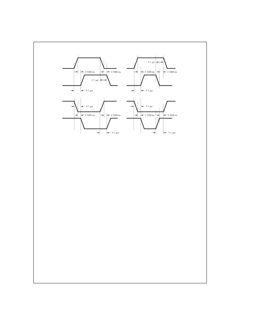
DS010568-24
FIGURE 4. Transitions in Brake, Direction, or PWM Must Be Separated By At Least 1 μsec
L
www.national.com
7
相關(guān)PDF資料 |
PDF描述 |
|---|---|
| LMD18201 | 3A, 55V H-Bridge |
| LMD18201T | 3A, 55V H-Bridge |
| LMD18245 | 3A, 55V DMOS Full-Bridge Motor Driver |
| LMD18245T | 3A, 55V DMOS Full-Bridge Motor Driver |
| LMD18400 | Quad High Side Driver |
相關(guān)代理商/技術(shù)參數(shù) |
參數(shù)描述 |
|---|---|
| LMD18200T | 制造商:Texas Instruments 功能描述:HALF BRIDGE 3A 55V 18200 SIL-11 |
| LMD18200T/HALF | 制造商:Texas Instruments 功能描述:HALF BRIDGE 3A 55V 18200 SIL-11 |
| LMD18200T/LB14 | 功能描述:馬達(dá)/運(yùn)動(dòng)/點(diǎn)火控制器和驅(qū)動(dòng)器 RoHS:否 制造商:STMicroelectronics 產(chǎn)品:Stepper Motor Controllers / Drivers 類(lèi)型:2 Phase Stepper Motor Driver 工作電源電壓:8 V to 45 V 電源電流:0.5 mA 工作溫度:- 25 C to + 125 C 安裝風(fēng)格:SMD/SMT 封裝 / 箱體:HTSSOP-28 封裝:Tube |
| LMD18200T/LF14 | 功能描述:馬達(dá)/運(yùn)動(dòng)/點(diǎn)火控制器和驅(qū)動(dòng)器 RoHS:否 制造商:STMicroelectronics 產(chǎn)品:Stepper Motor Controllers / Drivers 類(lèi)型:2 Phase Stepper Motor Driver 工作電源電壓:8 V to 45 V 電源電流:0.5 mA 工作溫度:- 25 C to + 125 C 安裝風(fēng)格:SMD/SMT 封裝 / 箱體:HTSSOP-28 封裝:Tube |
| LMD18200T/NOPB | 功能描述:馬達(dá)/運(yùn)動(dòng)/點(diǎn)火控制器和驅(qū)動(dòng)器 3A 55V H-Bridge RoHS:否 制造商:STMicroelectronics 產(chǎn)品:Stepper Motor Controllers / Drivers 類(lèi)型:2 Phase Stepper Motor Driver 工作電源電壓:8 V to 45 V 電源電流:0.5 mA 工作溫度:- 25 C to + 125 C 安裝風(fēng)格:SMD/SMT 封裝 / 箱體:HTSSOP-28 封裝:Tube |
發(fā)布緊急采購(gòu),3分鐘左右您將得到回復(fù)。