- 您現(xiàn)在的位置:買賣IC網(wǎng) > PDF目錄384603 > LMD18200 (National Semiconductor Corporation) 3A, 55V H-Bridge PDF資料下載
參數(shù)資料
| 型號: | LMD18200 |
| 廠商: | National Semiconductor Corporation |
| 英文描述: | 3A, 55V H-Bridge |
| 中文描述: | 第3A,55V的H橋 |
| 文件頁數(shù): | 6/13頁 |
| 文件大?。?/td> | 439K |
| 代理商: | LMD18200 |
Pinout Description
(See Connection Diagram) (Continued)
Pin 6, V
S
Power Supply
Pin 7, GROUND Connection:
This pin is the ground return,
and is internally connected to the mounting tab.
Pin 8, CURRENT SENSE Output:
This pin provides the
sourcing current sensing output signal, which is typically
377 μA/A.
Pin 9, THERMAL FLAG Output:
This pin provides the ther-
mal warning flag output signal. Pin 9 becomes active-low at
145C (junction temperature). However the chip will not shut
itself down until 170C is reached at the junction.
Pin 10, OUTPUT 2:
Half H-bridge number 2 output.
Pin 11, BOOTSTRAP 2 Input:
Bootstrap capacitor pin for
Half H-bridge number 2. The recommended capacitor
(10 nF) is connected between pins 10 and 11.
TABLE 1. Logic Truth Table
PWM
H
H
L
H
H
L
Dir
H
L
X
H
L
X
Brake
L
L
L
H
H
H
Active Output Drivers
Source 1, Sink 2
Sink 1, Source 2
Source 1, Source 2
Source 1, Source 2
Sink 1, Sink 2
NONE
Application Information
TYPES OF PWM SIGNALS
The LMD18200 readily interfaces with different forms of
PWM signals. Use of the part with two of the more popular
forms of PWM is described in the following paragraphs.
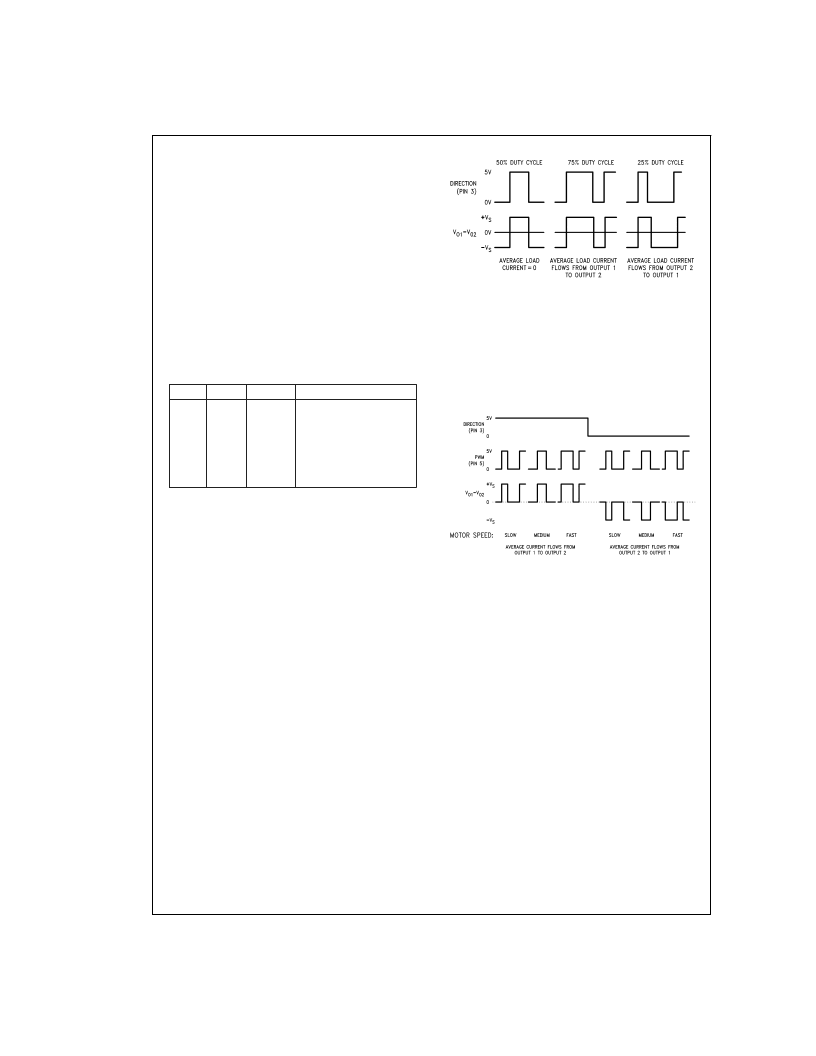
Simple, locked anti-phase PWM
consists of a single, vari-
able duty-cycle signal in which is encoded both direction and
amplitude information (see Figure 2). A 50% duty-cycle
PWM signal represents zero drive, since the net value of
voltage (integrated over one period) delivered to the load is
zero. For the LMD18200, the PWM signal drives the direc-
tion input (pin 3) and the PWM input (pin 5) is tied to logic
high.
Sign/magnitude PWM
consists of separate direction (sign)
and amplitude (magnitude) signals (see Figure 3). The (ab-
solute) magnitude signal is duty-cycle modulated, and the
absence of a pulse signal (a continuous logic low level) rep-
resents zero drive. Current delivered to the load is propor-
tional to pulse width. For the LMD18200, the DIRECTION in-
put (pin 3) is driven by the sign signal and the PWM input
(pin 5) is driven by the magnitude signal.
SIGNAL TRANSITION REQUIREMENTS
To ensure proper internal logic performance, it is good prac-
tice to avoid aligning the falling and rising edges of input sig-
nals. A delay of at least 1 μsec should be incorporated be-
tween transitions of the Direction, Brake, and/or PWM input
signals. A conservative approach is be sure there is at least
500ns delay between the end of the first transition and the
beginning of the second transition. See Figure 4
DS010568-4
FIGURE 2. Locked Anti-Phase PWM Control
DS010568-5
FIGURE 3. Sign/Magnitude PWM Control
L
www.national.com
6
相關(guān)PDF資料 |
PDF描述 |
|---|---|
| LMD18200T | 3A, 55V H-Bridge |
| LMD18201 | 3A, 55V H-Bridge |
| LMD18201T | 3A, 55V H-Bridge |
| LMD18245 | 3A, 55V DMOS Full-Bridge Motor Driver |
| LMD18245T | 3A, 55V DMOS Full-Bridge Motor Driver |
相關(guān)代理商/技術(shù)參數(shù) |
參數(shù)描述 |
|---|---|
| LMD18200_05 | 制造商:NSC 制造商全稱:National Semiconductor 功能描述:3A, 55V H-Bridge |
| LMD18200_13 | 制造商:TI 制造商全稱:Texas Instruments 功能描述:LMD18200 3A, 55V H-Bridge |
| LMD18200-2D/883 | 制造商:Texas Instruments 功能描述:H-Bridge DC Motor Driver 24-Pin SBCDIP Rail 制造商:Texas Instruments 功能描述:H-BRIDGE DC MOTOR DRVR 24PIN SBCDIP - Rail/Tube 制造商:Texas Instruments 功能描述:POWER MGNT DIV |
| LMD18200-2D-QV | 制造商:NSC 制造商全稱:National Semiconductor 功能描述:3A, 55V H-Bridge |
| LMD18200QML | 制造商:TI 制造商全稱:Texas Instruments 功能描述:2.4A, 55V H-Bridge |
發(fā)布緊急采購,3分鐘左右您將得到回復(fù)。