- 您現(xiàn)在的位置:買賣IC網(wǎng) > PDF目錄384602 > LMC2001AIMX (NATIONAL SEMICONDUCTOR CORP) High Precision, 6MHz Rail-To-Rail Output Operational Amplifier PDF資料下載
參數(shù)資料
| 型號: | LMC2001AIMX |
| 廠商: | NATIONAL SEMICONDUCTOR CORP |
| 元件分類: | 運動控制電子 |
| 英文描述: | High Precision, 6MHz Rail-To-Rail Output Operational Amplifier |
| 中文描述: | OP-AMP, 40 uV OFFSET-MAX, 6 MHz BAND WIDTH, PDSO8 |
| 封裝: | SOIC-8 |
| 文件頁數(shù): | 3/11頁 |
| 文件大小: | 430K |
| 代理商: | LMC2001AIMX |
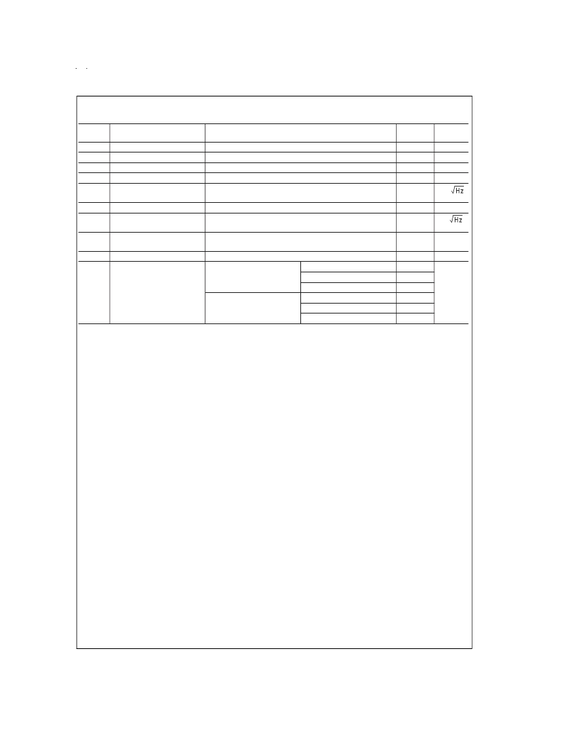
AC Electrical Characteristics
T
J
= 25C, V
+
= 5V, V
-
= 0V, V
CM
= 2.5V, V
O
= 2.5V, and R
L
>
1M
.
Symbol
Parameter
Conditions
Typ
(Note 5)
5
6
75
12
85
Units
SR
GBW
θ
m
G
m
e
n
Slew Rate
Gain-Bandwidth Product
Phase Margin
Gain Margin
Input-Referred Voltage Noise
A
V
= +1, V
in
=3.5Vpp
V/μs
MHz
Deg
dB
nV/
f = 0.1Hz
e
n
p-p
i
n
Input-Referred Voltage Noise
Input-Referred Current Noise
R
S
= 100
, DC to 10Hz
f = 0.1Hz
1.6
180
μVpp
fA/
THD
Total Harmonic Distortion
f = 1kHz, Av = -2
R
L
= 10k
,V
O
= 4.5Vpp
0.02
%
trec
T
S
Input Overload Recovery Time
Output Settling time
50
250
400
3200
80
860
1400
ms
ns
(Note 10) A
V
= +1, 1V step
1%
0.1%
0.01%
1%
0.1%
0.01%
(Note 10)A
V
= 1, 1V step
Note 1:
Absolute Maximum Ratings indicate limits beyond which damage to the device may occur. Operating Ratings indicate conditions for which the device is in-
tended to be functional, but specific performance is not guaranteed. For guaranteed specifications and test conditions, see the Electrical Characteristics.
Note 2:
Human body model, 1.5k
in series with 100pF. Machine model, 200
in series with 100pF.
Note 3:
Output currents in excess of
±
30mA over long term may adversely affect reliability.
Note 4:
The maximum power dissipation is a function of T
,
θ
, and T
A
. The maximum allowable power dissipation at any ambient temperature is P
D
= (T
J(max)
- T
A
)/
θ
JA
. All numbers apply for packages soldered directly onto a PC board.
Note 5:
Typical values represent the most likely parametric norm.
Note 6:
All limits are guaranteed by testing or statistical analysis, unless otherwise noted.
Note 7:
V
+
= 5V, V
CM
= 2.5V, and R
L
connected to 2.5V. For Sourcing tests, 2.5V
≤
V
O
≤
4.8V. For Sinking tests, 0.2V
≤
V
O
≤
2.5V.
Note 8:
Guaranteed Vos Drift is based on 280 devices operated for 1000 hrs at 150C (equivalent to 30 years 55oC).
Note 9:
Guaranteed by design only.
Note 10:
Settling times shown correspond to the worse case (positive or negative step) and does not include slew time. See the Application Note section for test
schematic.
Note 11:
The limits are set by the accuracy of high speed automatic test equipment. For the typical V
OS
distribution, see the curve on page 4.
Note 12:
Precision bench measurement of more than 300 units. More than 65% of units had less than 15nV /C V
OS
drift.
www.national.com
3
相關(guān)PDF資料 |
PDF描述 |
|---|---|
| LMC2626 | CMOS LDOR/Buffer Chip for Row Inversion Flat Panel Display Systems |
| LMC2626IM | CMOS LDOR/Buffer Chip for Row Inversion Flat Panel Display Systems |
| LMC272 | CMOS Dual Low Cost Rail to Rail Output Operational Amplifier |
| LMC272CM | CMOS Dual Low Cost Rail to Rail Output Operational Amplifier |
| LMC272CMM | CMOS Dual Low Cost Rail to Rail Output Operational Amplifier |
相關(guān)代理商/技術(shù)參數(shù) |
參數(shù)描述 |
|---|---|
| LMC200-2PS | 制造商:Black Box Corporation 功能描述:14 SLOT POWER CHASSIS W/2 POWE |
| LMC200-2PS-W1 | 制造商:Black Box Corporation 功能描述:1 YEAR WARRANTY FOR LMC200-2PS |
| LMC200-2PS-W3 | 制造商:Black Box Corporation 功能描述:3 YEAR WARRANTY FOR LMC200-2PS |
| LMC200A-2PS-DC | 制造商:Black Box Corporation 功能描述:FlexPoint 14-Slot Power Chassis, Dual DC Power Supplies |
| LMC200A-2PS-DC-W1 | 制造商:Black Box Corporation 功能描述:1 YEAR WARRANTY FOR LMC200A-2PS-DC |
發(fā)布緊急采購,3分鐘左右您將得到回復(fù)。