- 您現(xiàn)在的位置:買賣IC網 > PDF目錄385490 > LM94021BIMGX (National Semiconductor Corporation) Multi-Gain Analog Temperature Sensor PDF資料下載
參數(shù)資料
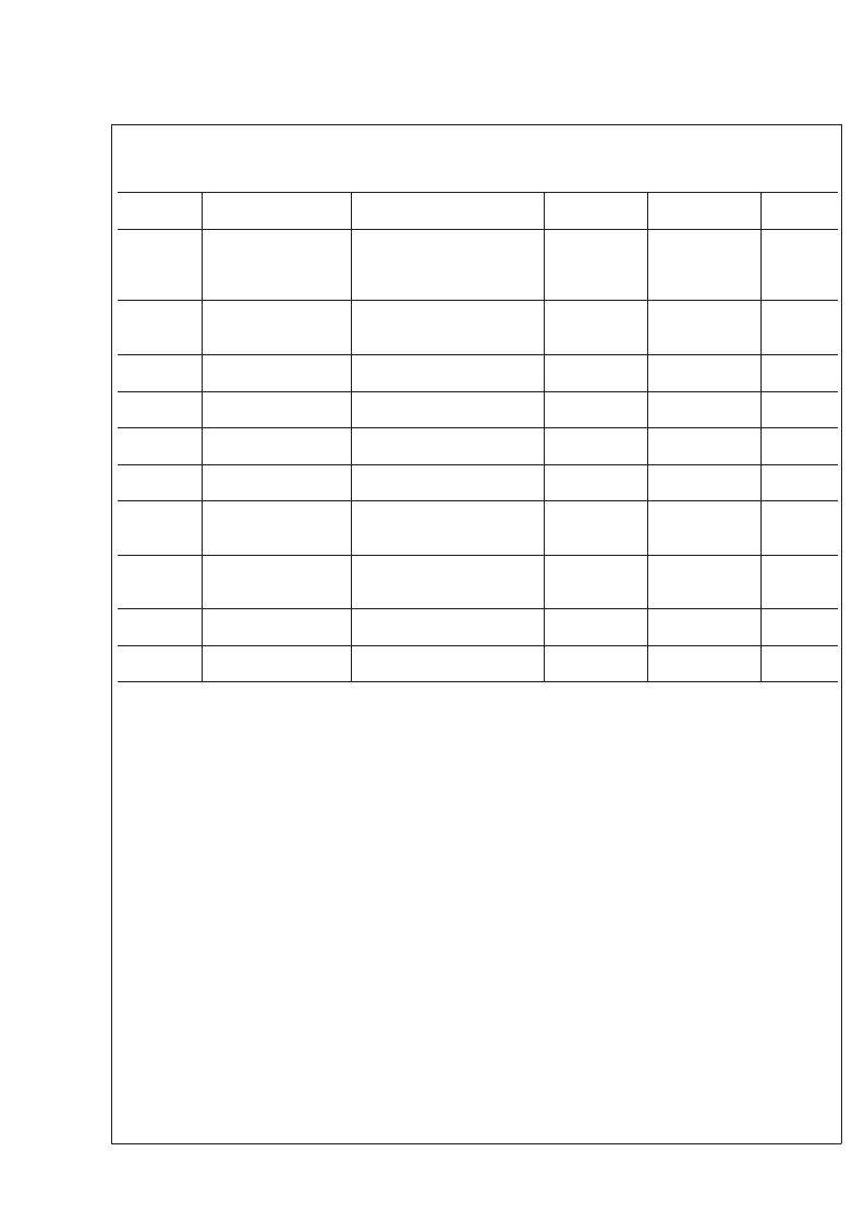
Electrical Characteristics
Unless otherwise noted, these specifications apply for +V
DD
= +1.5V to +5.5V .
Boldface limits apply for T
A
= T
J
= T
MIN
to
T
MAX
; all other limits T
A
= T
J
= 25C.
Symbol
Parameter
Conditions
Typical
(Note 6)
-5.5
-8.2
-10.9
-13.6
Limits
(Note 7)
Units
(Limit)
mV/C
mV/C
mV/C
mV/C
mV (max)
mV (max)
mV
μV/V
Sensor Gain
GS1 = 0, GS0 = 0
GS1 = 0, GS1 = 1
GS1 = 1, GS0 = 0
GS1 = 1, GS0 = 1
Source
≤
2.0 μA (Note 11)
Sink
≤
100 μA
Sink = 50 μA
(V
DD
- V
OUT
)
≥
200 mV
Load Regulation
(Note 10)
0.4
200
-1
1.6
Line Regulation (Note
14)
Supply Current
I
S
T
A
= +30C to +150C
T
A
= -50C to +150C
9
12
13
μA (max)
μA (max)
pF (max)
C
L
Output Load
Capacitance
Power-on Time
(Note 12)
GS1 and GS0 Input
Logic "1" Threshold
Voltage
GS1 and GS0 Input
Logic "0" Threshold
Voltage
Logic "1" Input Current
(Note 13)
Logic "0" Input Current
(Note 13)
1100
C
L
= 0 pF
C
L
=1100 pF
0.7
0.8
5
10
ms (max)
ms (max)
V (min)
V
IH
V
DD
- 0.5V
V
IL
0.5
V (max)
I
IH
0.001
1
μA (max)
I
IL
0.001
1
μA (max)
Note 1:
Absolute Maximum Ratings indicate limits beyond which damage to the device may occur. Operating Ratings indicate conditions for which the device is
functional, but do not guarantee specific performance limits. For guaranteed specifications and test conditions, see the Electrical Characteristics. The guaranteed
specifications apply only for the test conditions listed. Some performance characteristics may degrade when the device is not operated under the listed test
conditions.
Note 2:
When the input voltage (V
I
) at any pin exceeds power supplies (V
I
<
GND or V
I
>
V
+
), the current at that pin should be limited to 5 mA.
Note 3:
The human body model is a 100 pF capacitor discharged through a 1.5 k
resistor into each pin. The machine model is a 200 pF capacitor discharged
directly into each pin.
Note 4:
Reflow temperature profiles are different for lead-free and non-lead-free packages.
Note 5:
The junction to ambient thermal resistance (
θ
JA
) is specified without a heat sink in still air.
Note 6:
Typicals are at T
J
= T
A
= 25C and represent most likely parametric norm.
Note 7:
Limits are guaranteed to National’s AOQL (Average Outgoing Quality Level).
Note 8:
Accuracy is defined as the error between the measured and reference output voltages, tabulated in the Transfer Table at the specified conditions of supply
gain setting, voltage, and temperature (expressed in C). Accuracy limits include line regulation within the specified conditions. Accuracy limits do not include load
regulation; they assume no DC load.
Note 9:
Changes in output due to self heating can be computed by multiplying the internal dissipation by the thermal resistance.
Note 10:
Source currents are flowing out of the LM94021. Sink currents are flowing into the LM94021.
Note 11:
Assumes (V
DD
- V
OUT
)
^
200mV.
Note 12:
Guaranteed by design.
Note 13:
The input current is leakage only and is highest at high temperature. It is typically only 0.001μA. The 1μA limit is solely based on a testing limitation and
does not reflect the actual performance of the part.
Note 14:
Line regulation is calculated by subtracting the output voltage at the highest supply voltage from the output voltage at the lowest supply voltage. The typical
line regulation specification does not include the output voltage shift discussed in Section 5.0.
L
www.national.com
4
相關PDF資料 |
PDF描述 |
|---|---|
| LM94 | TruTherTM Hardware Monitor with PI Loop Fan Control for Server Management |
| LM94CIMT | TruTherTM Hardware Monitor with PI Loop Fan Control for Server Management |
| LM94CIMTX | TruTherTM Hardware Monitor with PI Loop Fan Control for Server Management |
| LM95231 | TruTherm Precision Dual Remote Diode Temperature Sensor with SMBus Interface |
| LM95233 | Dual Remote Diode and Local Temperature Sensor with SMBus Interface, TCRITs and TruTherm⑩ Technology |
相關代理商/技術參數(shù) |
參數(shù)描述 |
|---|---|
| LM94021BIMGX/NOPB | 功能描述:板上安裝溫度傳感器 RoHS:否 制造商:Omron Electronics 輸出類型:Digital 配置: 準確性:+/- 1.5 C, +/- 3 C 溫度閾值: 數(shù)字輸出 - 總線接口:2-Wire, I2C, SMBus 電源電壓-最大:5.5 V 電源電壓-最小:4.5 V 最大工作溫度:+ 50 C 最小工作溫度:0 C 關閉: 安裝風格: 封裝 / 箱體: 設備功能:Temperature and Humidity Sensor |
| LM94021EVAL | 功能描述:溫度傳感器開發(fā)工具 LM94021 EVAL BOARD RoHS:否 制造商:Texas Instruments 產品類型:Temperature Sensors and Control ICs 工具用于評估:MSP430G2553 接口類型:USB 工作電源電壓: 工作電源電流: |
| LM94021QBIMG/NOPB | 功能描述:板上安裝溫度傳感器 Analog Temp Sensor RoHS:否 制造商:Omron Electronics 輸出類型:Digital 配置: 準確性:+/- 1.5 C, +/- 3 C 溫度閾值: 數(shù)字輸出 - 總線接口:2-Wire, I2C, SMBus 電源電壓-最大:5.5 V 電源電壓-最小:4.5 V 最大工作溫度:+ 50 C 最小工作溫度:0 C 關閉: 安裝風格: 封裝 / 箱體: 設備功能:Temperature and Humidity Sensor |
| LM94021QBIMGX/NOPB | 功能描述:板上安裝溫度傳感器 RoHS:否 制造商:Omron Electronics 輸出類型:Digital 配置: 準確性:+/- 1.5 C, +/- 3 C 溫度閾值: 數(shù)字輸出 - 總線接口:2-Wire, I2C, SMBus 電源電壓-最大:5.5 V 電源電壓-最小:4.5 V 最大工作溫度:+ 50 C 最小工作溫度:0 C 關閉: 安裝風格: 封裝 / 箱體: 設備功能:Temperature and Humidity Sensor |
| LM94022 | 制造商:NSC 制造商全稱:National Semiconductor 功能描述:1.5V, SC70, Multi-Gain Analog Temperature Sensor with Class-AB Output |
發(fā)布緊急采購,3分鐘左右您將得到回復。