- 您現(xiàn)在的位置:買賣IC網(wǎng) > PDF目錄98000 > LM2984MDC (NATIONAL SEMICONDUCTOR CORP) 1-CHANNEL POWER SUPPLY SUPPORT CKT, UUC PDF資料下載
參數(shù)資料
| 型號: | LM2984MDC |
| 廠商: | NATIONAL SEMICONDUCTOR CORP |
| 元件分類: | 電源管理 |
| 英文描述: | 1-CHANNEL POWER SUPPLY SUPPORT CKT, UUC |
| 封裝: | DIE |
| 文件頁數(shù): | 3/16頁 |
| 文件大?。?/td> | 317K |
| 代理商: | LM2984MDC |
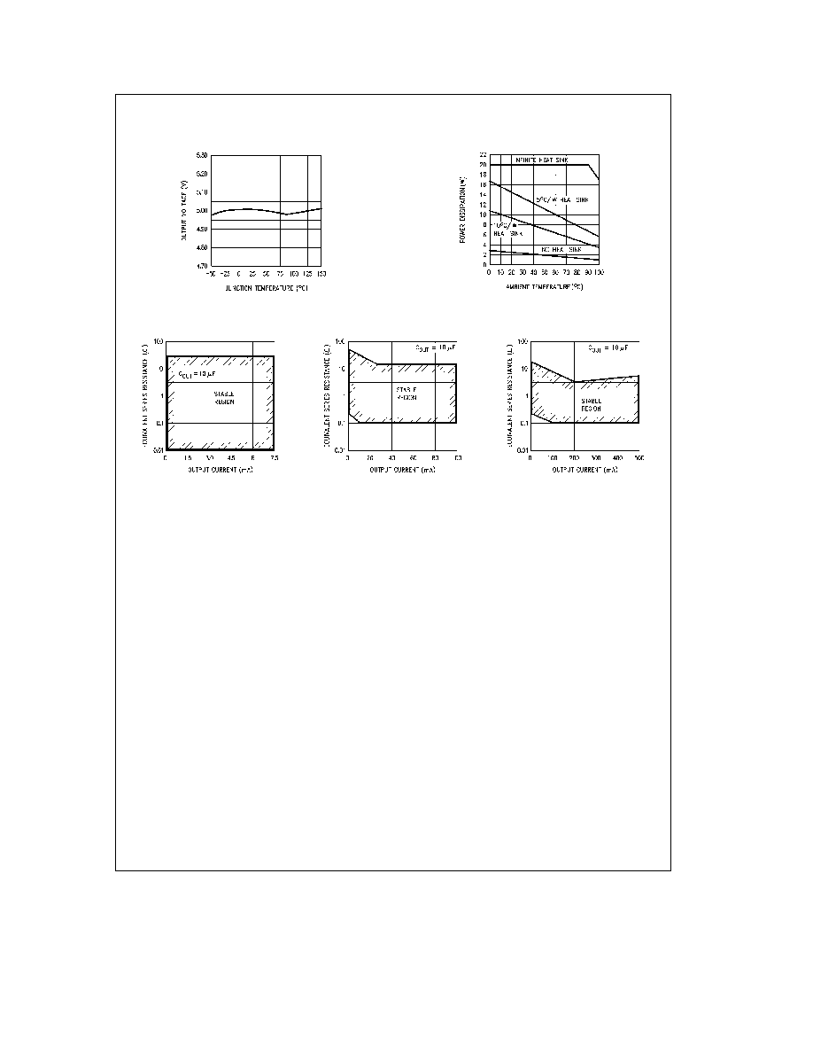
Typical Performance Characteristics (Continued)
Output Voltage
TLH8821 – 8
Device Dissipation vs
Ambient Temperature
TLH8821 – 9
Output Capacitor ESR
(Standby Output Pin 9)
TLH8821 – 13
Output Capacitor ESR
(Buffer Output Pin 10)
TLH8821 – 14
Output Capacitor ESR
(Main Output Pin 11)
TLH8821 – 15
Application Hints
OUTPUT CAPACITORS
The LM2984C output capacitors are required for stability
Without them the regulator outputs will oscillate sometimes
by many volts Though the 10 mF shown are the minimum
recommended values actual size and type may vary de-
pending upon the application load and temperature range
Capacitor effective series resistance (ESR) also affects the
IC stability Since ESR varies from one brand to the next
some bench work may be required to determine the mini-
mum capacitor value to use in production Worst case is
usually determined at the minimum ambient temperature
and the maximum load expected
Output capacitors can be increased in size to any desired
value above the minimum One possible purpose of this
would be to maintain the output voltages during brief condi-
tions of negative input transients that might be characteris-
tic of a particular system
Capacitors must also be rated at all ambient temperatures
expected in the system Many aluminum type electrolytics
will freeze at temperatures less than b30 C reducing their
effective capacitance to zero To maintain regulator stability
down to b40 C capacitors rated at that temperature (such
as tantalums) must be used
Each output must be terminated by a capacitor even if it is
not used
STANDBY OUTPUT
The standby output is intended for use in systems requiring
standby memory circuits While the high current regulator
outputs are controlled with the ONOFF pin described later
the standby output remains on under all conditions as long
as sufficient input voltage is supplied to the IC Thus memo-
ry and other circuits powered by this output remain unaffect-
ed by positive line transients thermal shutdown etc
The standby regulator circuit is designed so that the quies-
cent current to the IC is very low (k15 mA) when the other
regulator outputs are off
The capacitor on the output of this regulator can be in-
creased without bound This will help maintain the output
voltage during negative input transients and will also help to
reduce the noise on all three outputs Because the other
two track the standby output therefore any noise reduction
here will also reduce the other two noise voltages
BUFFER OUTPUT
The buffer output is designed to drive peripheral sensor cir-
cuitry in a mP system It will track the standby and main
regulator within a few millivolts in normal operation There-
fore a peripheral sensor can be powered off this supply and
have the same operating voltage as the mP system This is
important if a ratiometric sensor system is being used
The buffer output can be short circuited while the other two
outputs are in normal operation This protects the mP sys-
tem from disruption of power when a sensor wire etc is
temporarily shorted to ground ie only the sensor signal
would be interrupted while the mP and memory circuits
would remain operational
The buffer output is similar to the main output in that it is
controlled by the ONOFF switch in order to save power in
11
相關(guān)PDF資料 |
PDF描述 |
|---|---|
| LM3207TL/NOPB | 1.2 A SWITCHING REGULATOR, 2300 kHz SWITCHING FREQ-MAX, PBGA9 |
| LM3218SE | SWITCHING REGULATOR, DSO8 |
| LM3350MWC | SWITCHED CAPACITOR CONVERTER, 1100 kHz SWITCHING FREQ-MAX, UUC |
| LM336BZ-5.0/NOPB | 1-OUTPUT TWO TERM VOLTAGE REFERENCE, 5 V, PBCY3 |
| LM336Z-2.5/T7 | 1-OUTPUT TWO TERM VOLTAGE REFERENCE, 2.49 V, PBCY3 |
相關(guān)代理商/技術(shù)參數(shù) |
參數(shù)描述 |
|---|---|
| LM2984T | 功能描述:低壓差穩(wěn)壓器 - LDO RoHS:否 制造商:Texas Instruments 最大輸入電壓:36 V 輸出電壓:1.4 V to 20.5 V 回動電壓(最大值):307 mV 輸出電流:1 A 負(fù)載調(diào)節(jié):0.3 % 輸出端數(shù)量: 輸出類型:Fixed 最大工作溫度:+ 125 C 安裝風(fēng)格:SMD/SMT 封裝 / 箱體:VQFN-20 |
| LM2984T/NOPB | 功能描述:低壓差穩(wěn)壓器 - LDO RoHS:否 制造商:Texas Instruments 最大輸入電壓:36 V 輸出電壓:1.4 V to 20.5 V 回動電壓(最大值):307 mV 輸出電流:1 A 負(fù)載調(diào)節(jié):0.3 % 輸出端數(shù)量: 輸出類型:Fixed 最大工作溫度:+ 125 C 安裝風(fēng)格:SMD/SMT 封裝 / 箱體:VQFN-20 |
| LM2990J-12-QML | 制造商:National Semiconductor Corporation 功能描述:LDO Regulator Neg -12V 1.8A 16-Pin CDIP Tray 制造商:National Semiconductor 功能描述:LDO Regulator Neg -12V 1.8A 16-Pin CDIP Tray |
| LM2990J-15-QML | 制造商:Texas Instruments 功能描述:LDO Regulator Neg -15V 1.8A 16-Pin CDIP Tray |
| LM2990J-5.0-QM | 制造商:National Semiconductor Corporation 功能描述:LDO Regulator Neg -5V 1.8A 16-Pin CDIP Rail 制造商:National Semiconductor 功能描述:LDO Regulator Neg -5V 1.8A 16-Pin CDIP Rail |
發(fā)布緊急采購,3分鐘左右您將得到回復(fù)。