- 您現(xiàn)在的位置:買賣IC網(wǎng) > PDF目錄385477 > LM2765 (National Semiconductor Corporation) Switched Capacitor Voltage Converter PDF資料下載
參數(shù)資料
| 型號: | LM2765 |
| 廠商: | National Semiconductor Corporation |
| 元件分類: | 基準電壓源/電流源 |
| 英文描述: | Switched Capacitor Voltage Converter |
| 中文描述: | 開關電容電壓轉(zhuǎn)換器 |
| 文件頁數(shù): | 6/9頁 |
| 文件大?。?/td> | 208K |
| 代理商: | LM2765 |

Circuit Description
The LM2765 contains four large CMOS switches which are
switched in a sequence to double the input supply voltage.
Energy transfer and storage are provided by external capaci-
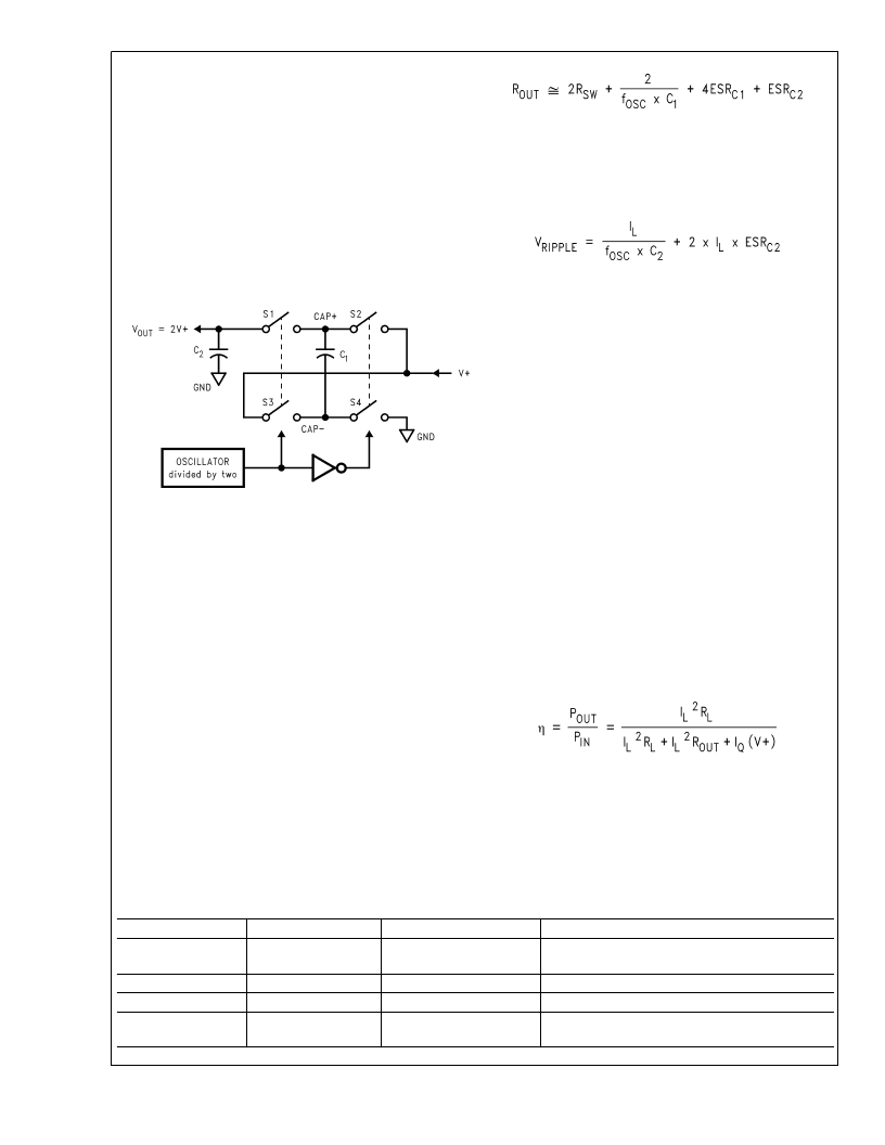
tors. Figure 2 illustrates the voltage conversion scheme.
When S
2
and S
4
are closed, C
1
charges to the supply volt-
age V+. During this time interval, switches S
and S
are
open. In the next time interval, S
and S
are open; at the
same time, S
and S
are closed, the sum of the input volt-
age V+ and the voltage across C
gives the 2V+ output volt-
age when there is no load. The output voltage drop when a
load is added is determined by the parasitic resistance (R
d-
s(on)
of the MOSFET switches and the ESR of the capacitors)
and the charge transfer loss between capacitors. Details will
be discussed in the following application information section.
Application Information
Positive Voltage Doubler
The main application of the LM2765 is to double the input
voltage. The range of the input supply voltage is 1.8V to
5.5V.
The output characteristics of this circuit can be approximated
by an ideal voltage source in series with a resistance. The
voltage source equals 2V+. The output resistance R
is a
function of the ON resistance of the internal MOSFET
switches, the oscillator frequency, and the capacitance and
ESR of C
and C
. Since the switching current charging and
discharging C
is approximately twice as the output current,
the effect of the ESR of the pumping capacitor C
will be
multiplied by four in the output resistance. The output ca-
pacitor C
is charging and discharging at a current approxi-
mately equal to the output current, therefore, its ESR only
counts once in the output resistance. A good approximation
of R
out
is:
where R
is the sum of the ON resistance of the internal
MOSFET switches shown in Figure 2. R
SW
is typically 8
for
the LM2765.
The peak-to-peak output voltage ripple is determined by the
oscillator frequency as well as the capacitance and ESR of
the output capacitor C
2
:
High capacitance, low ESR capacitors can reduce both the
output resistance and the voltage ripple.
The Schottky diode D
is only needed to protect the device
from turning-on its own parasitic diode and potentially
latching-up. During start-up, D
will also quickly charge up
the output capacitor to V
minus the diode drop thereby de-
creasing the start-up time. Therefore, the Schottky diode D
1
should have enough current carrying capability to charge the
output capacitor at start-up, as well as a low forward voltage
to prevent the internal parasitic diode from turning-on. A
Schottky diode like 1N5817 can be used for most applica-
tions. If the input voltage ramp is less than 10V/ms, a smaller
Schottky diode like MBR0520LT1 can be used to reduce the
circuit size.
Shutdown Mode
A shutdown (SD) pin is available to disable the device and
reduce the quiescent current to 0.1 μA. In normal operating
mode, the SD pin is connected to ground. The device can be
brought into the shutdown mode by applying to the SD pin a
voltage greater than 40% of the V+ pin voltage.
Capacitor Selection
As discussed in the Positive Voltage Doubler section, the
output resistance and ripple voltage are dependent on the
capacitance and ESR values of the external capacitors. The
output voltage drop is the load current times the output resis-
tance, and the power efficiency is
Where I
Q
(V+) is the quiescent power loss of the IC device,
and I
L2
R
is the conversion loss associated with the switch
on-resistance, the two external capacitors and their ESRs.
The selection of capacitors is based on the specifications of
the dropout voltage (which equals I
R
), the output volt-
age ripple, and the converter efficiency. Low ESR capacitors
(Table 1) are recommended to maximize efficiency, reduce
the output voltage drop and voltage ripple.
TABLE 1. Low ESR Capacitor Manufacturers
Manufacturer
Nichicon Corp.
Phone
Website
Capacitor Type
(847)-843-7500
www.nichicon.com
PL & PF series, through-hole aluminum
electrolytic
TPS series, surface-mount tantalum
593D, 594D, 595D series, surface-mount tantalum
OS-CON series, through-hole aluminum
electrolytic
AVX Corp.
Sprague
Sanyo
(843)-448-9411
(207)-324-4140
(619)-661-6835
www.avxcorp.com
www.vishay.com
www.sanyovideo.com
DS101281-14
FIGURE 2. Voltage Doubling Principle
L
www.national.com
6
相關PDF資料 |
PDF描述 |
|---|---|
| LM2765M6 | Switched Capacitor Voltage Converter |
| LM2765M6X | Switched Capacitor Voltage Converter |
| LM2781 | Ultra-Low Ripple Switched Capacitor Voltage Inverter |
| LM2781TP | Ultra-Low Ripple Switched Capacitor Voltage Inverter |
| LM2781TPX | Ultra-Low Ripple Switched Capacitor Voltage Inverter |
相關代理商/技術參數(shù) |
參數(shù)描述 |
|---|---|
| LM2765M6 | 制造商:Rochester Electronics LLC 功能描述: 制造商:Texas Instruments 功能描述: |
| LM2765M6/NOPB | 功能描述:IC REG SWITCHED CAP DBL SOT23-6 RoHS:是 類別:集成電路 (IC) >> PMIC - 穩(wěn)壓器 - DC DC 開關穩(wěn)壓器 系列:- 產(chǎn)品培訓模塊:Lead (SnPb) Finish for COTS Obsolescence Mitigation Program 標準包裝:1 系列:- 類型:降壓(降壓) 輸出類型:固定 輸出數(shù):1 輸出電壓:3.3V 輸入電壓:4.5 V ~ 24 V PWM 型:- 頻率 - 開關:- 電流 - 輸出:125mA 同步整流器:無 工作溫度:-40°C ~ 85°C 安裝類型:表面貼裝 封裝/外殼:SOT-23-6 包裝:Digi-Reel® 供應商設備封裝:SOT-6 其它名稱:MAX1836EUT33#TG16DKR |
| LM2765M6X | 功能描述:電荷泵 RoHS:否 制造商:Maxim Integrated 功能:Inverting, Step Up 輸出電壓:- 1.5 V to - 5.5 V, 3 V to 11 V 輸出電流:100 mA 電源電流:1 mA 最大工作溫度:+ 70 C 封裝 / 箱體:SOIC-8 Narrow 封裝:Tube |
| LM2765M6X/NOPB | 功能描述:電荷泵 RoHS:否 制造商:Maxim Integrated 功能:Inverting, Step Up 輸出電壓:- 1.5 V to - 5.5 V, 3 V to 11 V 輸出電流:100 mA 電源電流:1 mA 最大工作溫度:+ 70 C 封裝 / 箱體:SOIC-8 Narrow 封裝:Tube |
| LM2766 | 制造商:NSC 制造商全稱:National Semiconductor 功能描述:Switched Capacitor Voltage Converter |
發(fā)布緊急采購,3分鐘左右您將得到回復。