- 您現(xiàn)在的位置:買賣IC網(wǎng) > PDF目錄44548 > LM2586-ADJMDC (NATIONAL SEMICONDUCTOR CORP) 7 A SWITCHING REGULATOR, 200 kHz SWITCHING FREQ-MAX, UUC PDF資料下載
參數(shù)資料
| 型號: | LM2586-ADJMDC |
| 廠商: | NATIONAL SEMICONDUCTOR CORP |
| 元件分類: | 穩(wěn)壓器 |
| 英文描述: | 7 A SWITCHING REGULATOR, 200 kHz SWITCHING FREQ-MAX, UUC |
| 封裝: | DIE |
| 文件頁數(shù): | 16/32頁 |
| 文件大?。?/td> | 858K |
| 代理商: | LM2586-ADJMDC |
第1頁第2頁第3頁第4頁第5頁第6頁第7頁第8頁第9頁第10頁第11頁第12頁第13頁第14頁第15頁當(dāng)前第16頁第17頁第18頁第19頁第20頁第21頁第22頁第23頁第24頁第25頁第26頁第27頁第28頁第29頁第30頁第31頁第32頁
Application Hints (Continued)
stable or constant voltage supply to the LM2586, a storage
capacitor (
≥100 F) is required. If the input source is a recti-
fied DC supply and/or the application has a wide tempera-
ture range, the required rms current rating of the capacitor
might be very large. This means a larger value of capaci-
tance or a higher voltage rating will be needed for the input
capacitor. The storage capacitor will also attenuate noise
which may interfere with other circuits connected to the
same input supply voltage.
In addition, a small bypass capacitor is required due to the
noise generated by the input current pulses. To eliminate the
noise, insert a 1.0 F ceramic capacitor between V
IN and
ground as close as possible to the device.
SWITCH VOLTAGE LIMITS
In a flyback regulator, the maximum steady-state voltage ap-
pearing at the switch, when it is off, is set by the transformer
turns ratio, N, the output voltage, V
OUT, and the maximum in-
put voltage, V
IN (Max):
V
SW(OFF) = VIN (Max) + (VOUT +VF)/N
where V
F is the forward biased voltage of the output diode,
and is typically 0.5V for Schottky diodes and 0.8V for
ultra-fast recovery diodes. In certain circuits, there exists a
voltage spike, V
LL, superimposed on top of the steady-state
voltage (see
Figure 5, waveform A). Usually, this voltage
spike is caused by the transformer leakage inductance
and/or the output rectifier recovery time. To “clamp” the volt-
age at the switch from exceeding its maximum value, a tran-
sient suppressor in series with a diode is inserted across the
transformer primary (as shown in the circuit in
Figure 4 and
other flyback regulator circuits throughout the datasheet).
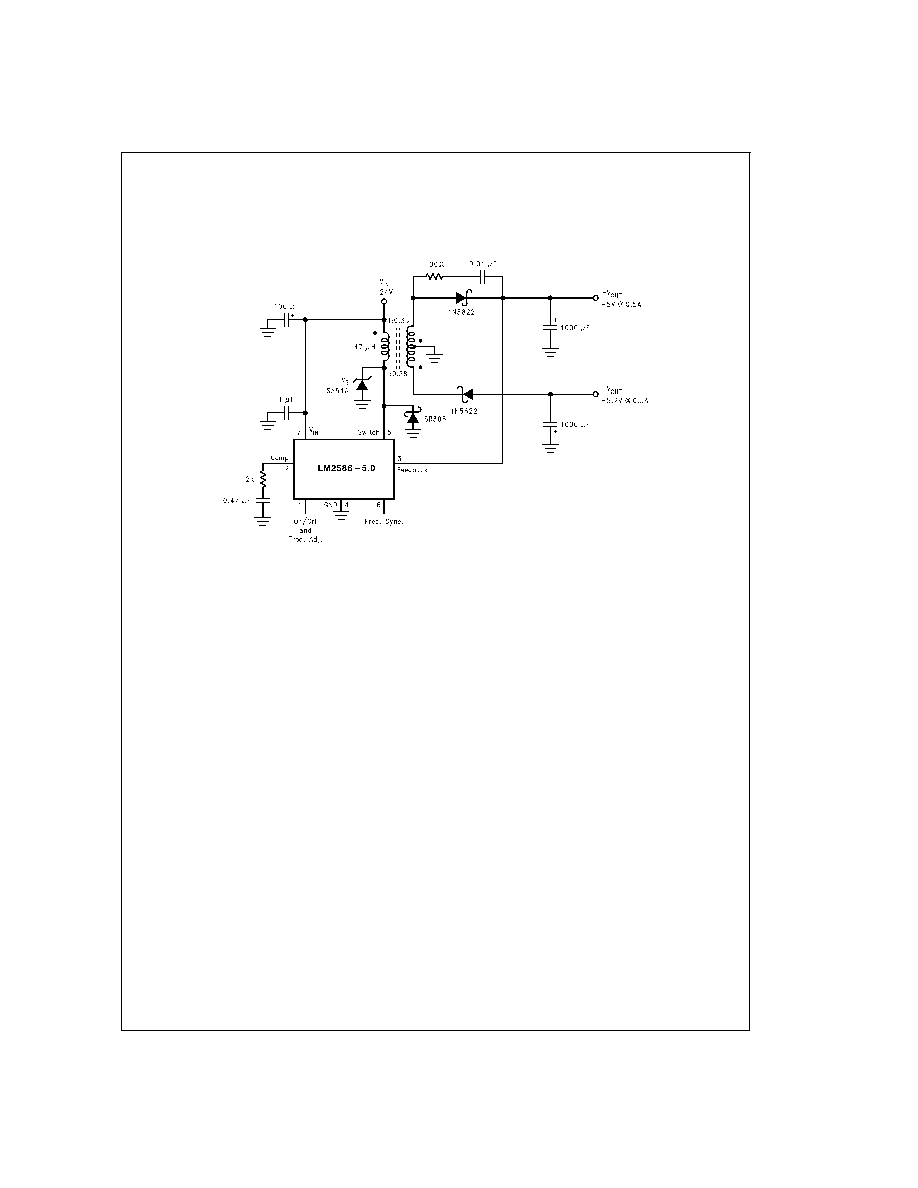
The schematic in
Figure 43 shows another method of clamp-
ing the switch voltage. A single voltage transient suppressor
(the SA51A) is inserted at the switch pin. This method
clamps the total voltage across the switch, not just the volt-
age across the primary.
If poor circuit layout techniques are used (see the “Circuit
Layout Guideline” section), negative voltage transients may
appear on the Switch pin (pin 5). Applying a negative voltage
(with respect to the IC’s ground) to any monolithic IC pin
causes erratic and unpredictable operation of that IC. This
holds true for the LM2586 IC as well. When used in a flyback
regulator, the voltage at the Switch pin (pin 5) can go nega-
tive when the switch turns on. The “ringing” voltage at the
switch pin is caused by the output diode capacitance and the
transformer leakage inductance forming a resonant circuit at
the secondary(ies). The resonant circuit generates the “ring-
ing” voltage, which gets reflected back through the trans-
former to the switch pin. There are two common methods to
avoid this problem. One is to add an RC snubber around the
output rectifier(s), as in
Figure 43. The values of the resistor
and the capacitor must be chosen so that the voltage at the
Switch pin does not drop below 0.4V. The resistor may
range in value between 10
and1k, and the capacitor will
vary from 0.001 F to 0.1 F. Adding a snubber will (slightly)
reduce the efficiency of the overall circuit.
The other method to reduce or eliminate the “ringing” is to in-
sert a Schottky diode clamp between pins 5 and 4 (ground),
also shown in
Figure 43. This prevents the voltage at pin 5
from dropping below 0.4V. The reverse voltage rating of the
diode must be greater than the switch off voltage.
DS012516-62
FIGURE 43. Flyback Regulator
www.national.com
23
相關(guān)PDF資料 |
PDF描述 |
|---|---|
| LM2586SX-12/NOPB | 3 A SWITCHING REGULATOR, 200 kHz SWITCHING FREQ-MAX, PSSO7 |
| LM2587SX-3.3/NOPB | 5 A SWITCHING REGULATOR, 100 kHz SWITCHING FREQ-MAX, PSSO5 |
| LM2588-12MWC | 9.5 A SWITCHING REGULATOR, 200 kHz SWITCHING FREQ-MAX, UUC |
| LM2588-12MDC | 9.5 A SWITCHING REGULATOR, 200 kHz SWITCHING FREQ-MAX, UUC |
| LM2588-ADJMWC | 9.5 A SWITCHING REGULATOR, 200 kHz SWITCHING FREQ-MAX, UUC |
相關(guān)代理商/技術(shù)參數(shù) |
參數(shù)描述 |
|---|---|
| LM2586S-12 | 功能描述:直流/直流開關(guān)轉(zhuǎn)換器 RoHS:否 制造商:STMicroelectronics 最大輸入電壓:4.5 V 開關(guān)頻率:1.5 MHz 輸出電壓:4.6 V 輸出電流:250 mA 輸出端數(shù)量:2 最大工作溫度:+ 85 C 安裝風(fēng)格:SMD/SMT |
| LM2586S-12/NOPB | 功能描述:直流/直流開關(guān)轉(zhuǎn)換器 RoHS:否 制造商:STMicroelectronics 最大輸入電壓:4.5 V 開關(guān)頻率:1.5 MHz 輸出電壓:4.6 V 輸出電流:250 mA 輸出端數(shù)量:2 最大工作溫度:+ 85 C 安裝風(fēng)格:SMD/SMT |
| LM2586S-3.3 | 功能描述:直流/直流開關(guān)轉(zhuǎn)換器 RoHS:否 制造商:STMicroelectronics 最大輸入電壓:4.5 V 開關(guān)頻率:1.5 MHz 輸出電壓:4.6 V 輸出電流:250 mA 輸出端數(shù)量:2 最大工作溫度:+ 85 C 安裝風(fēng)格:SMD/SMT |
| LM2586S-3.3/NOPB | 功能描述:直流/直流開關(guān)轉(zhuǎn)換器 RoHS:否 制造商:STMicroelectronics 最大輸入電壓:4.5 V 開關(guān)頻率:1.5 MHz 輸出電壓:4.6 V 輸出電流:250 mA 輸出端數(shù)量:2 最大工作溫度:+ 85 C 安裝風(fēng)格:SMD/SMT |
| LM2586S-5.0 | 功能描述:直流/直流開關(guān)轉(zhuǎn)換器 RoHS:否 制造商:STMicroelectronics 最大輸入電壓:4.5 V 開關(guān)頻率:1.5 MHz 輸出電壓:4.6 V 輸出電流:250 mA 輸出端數(shù)量:2 最大工作溫度:+ 85 C 安裝風(fēng)格:SMD/SMT |
發(fā)布緊急采購,3分鐘左右您將得到回復(fù)。