- 您現(xiàn)在的位置:買賣IC網(wǎng) > PDF目錄30743 > LM1269NA/NOPB (NATIONAL SEMICONDUCTOR CORP) 3 CHANNEL, VIDEO PREAMPLIFIER, PDIP24 PDF資料下載
參數(shù)資料
| 型號(hào): | LM1269NA/NOPB |
| 廠商: | NATIONAL SEMICONDUCTOR CORP |
| 元件分類: | 音頻/視頻放大 |
| 英文描述: | 3 CHANNEL, VIDEO PREAMPLIFIER, PDIP24 |
| 封裝: | PLASTIC, DIP-24 |
| 文件頁(yè)數(shù): | 15/20頁(yè) |
| 文件大小: | 1676K |
| 代理商: | LM1269NA/NOPB |
第1頁(yè)第2頁(yè)第3頁(yè)第4頁(yè)第5頁(yè)第6頁(yè)第7頁(yè)第8頁(yè)第9頁(yè)第10頁(yè)第11頁(yè)第12頁(yè)第13頁(yè)第14頁(yè)當(dāng)前第15頁(yè)第16頁(yè)第17頁(yè)第18頁(yè)第19頁(yè)第20頁(yè)
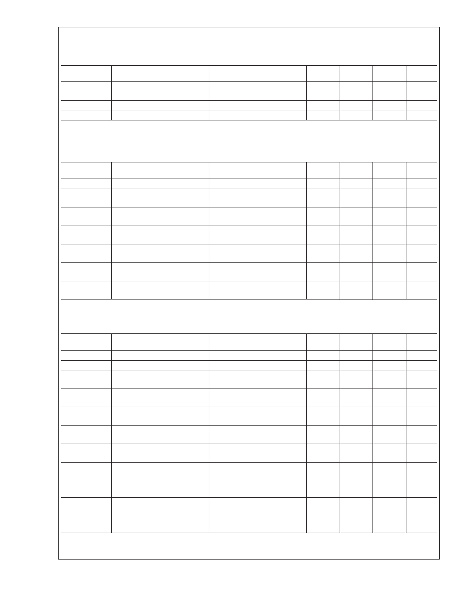
OSD Electrical Characteristics (Continued)
Unless otherwise noted: T
A = 25C, VCC = +5V, VIN = 0.7V, VABL =VCC,CL = 8 pF, Video Signal Output = 2 VP-P, Test Set-
ting 8.
Symbol
Parameter
Conditions
Min
(Note 7)
Typ
(Note 6)
Max
(Note 7)
Units
t
OSD/OSD S
Output Skew Time between
OSD and OSD Select
Measured from 50% Point on
all Waveforms
±2.0
ns
V
feed 10 kHz
Video Feedthrough into OSD
OSD Inputs = 0V
70
dB
V
feed 10 MHz
Video Feedthrough into OSD
OSD Inputs = 0V
60
dB
External DAC Signals Electrical Characteristics
Unless otherwise noted: T
A = 25C, VCC = +5V, VIN = 0.7V, VABL =VCC,CL = 8 pF, Video Signal Output = 2 VP-P. The fol-
lowing apply for all four external DACs.
Symbol
Parameter
Conditions
Min
(Note 7)
Typ
(Note 6)
Max
(Note 7)
Units
V
Min DAC
Min DAC Output Voltage
Value = 00h
0.5
0.75
V
Max DAC
Mode 00
Max DAC Output Voltage
Value = FFh, DCF[1:0] = 00h
(no load)
3.6
4.2
V
Max DAC
Mode 11
Max Output Voltage of DACs
1–3 in DCF Mode 11
Value = FFh, DCF[1:0] = 11h,
DAC4 Value = 00h
1.85
2.1
2.35
V
Max DAC
(Temp)
Variation of any DAC output
voltage with temperature
0C<T<70C ambient
±0.5
mV/deg
V
Max DAC
(V
CC)
Variation of any DAC output
voltage with V
CC
4.75V<V
CC<5.25V
±50
mV/V
Linearity
Linearity of DAC Over its
Range
5%
Monotonicity
Monotonicity of the DAC
Excluding dead zones at limits
of DAC
±0.5
LSB
External Interface Signals Electrical Characteristics
Unless otherwise noted: T
A = 25C, VCC = +5V, VIN = 0.7V, VABL =VCC,CL = 8 pF, Video Output = 2 VP-P.
Symbol
Parameter
Conditions
Min
(Note 7)
Typ
(Note 6)
Max
(Note 7)
Units
V
l(I
2C)
I
2C Low Input Voltage
SDA or SCL Inputs
0.5
1.5
V
h(I
2C)
I
2C High Input Voltage
SDA or SCL Inputs
3.0
4.0
5.0
V
I
l(I
2C)
I
2C Low Input Current
SDA or SCL Inputs, Input
Voltage = 0V
1.9
2.2
2.5
A
I
h(I
2C)
I
2C High Input Current
SDA or SCL Inputs, Input
Voltage = 5V
0.3
0.6
0.9
A
t
H-Blank on
H-Blank Time Delay from Zero
Crossing Point of H Flyback
Rising Edge of the Flyback
Signal
50
ns
t
H-Blank off
H-Blank Time Delay from Zero
Crossing Point of H Flyback
Falling Edge of the Flyback
Signal
50
ns
I
In Threshold
I
In H-Blank Detection
Threshold
20
A
I
In-Operating
Minimum — Insure Normal
Operation
Maximum — Should Not
Exceed in Normal Operation
Lowest Operating Horizontal
Frequency in Given Application
(Note 17)
30
300
A
I
In Flyback
Peak Current during Flyback
Period, Recommended Design
Range
Operating Range for all
Horizontal Scan Frequencies,
Maximum Current Should Not
Exceed 2 mA (Note 17)
0.5
1.5
2.0
mA
Note 1: Limits of Absolute Maximum Ratings indicate limits below which damage to the device must not occur.
Note 2: Limits of operating ratings indicate required boundaries of conditions for which the device is functional, but may not meet specific performance limits.
LM1269
www.national.com
4
相關(guān)PDF資料 |
PDF描述 |
|---|---|
| LM1276AAA/NA | 1 CHANNEL, VIDEO PREAMPLIFIER, PDIP28 |
| LM1279AN/NOPB | 3 CHANNEL, VIDEO AMPLIFIER, PDIP20 |
| LM1279N/NOPB | 1 CHANNEL, VIDEO AMPLIFIER, PDIP20 |
| LM136A-2.5MD8 | 1-OUTPUT TWO TERM VOLTAGE REFERENCE, 5 V, UUC |
| LM136A-5.0MW8 | 1-OUTPUT TWO TERM VOLTAGE REFERENCE, 5 V, UUC |
相關(guān)代理商/技術(shù)參數(shù) |
參數(shù)描述 |
|---|---|
| LM126H | 制造商:NSC 制造商全稱:National Semiconductor 功能描述:VOLTAGE REGULATORS |
| LM126H/883B | 制造商:Texas Instruments 功能描述:IC,VOLT REGULATOR,FIXED,+-12V,BIPOLAR,CAN,10PIN,METAL |
| LM126H/883C | 制造商:Texas Instruments 功能描述: |
| LM1270 | 制造商:NSC 制造商全稱:National Semiconductor 功能描述:Hi-Brite 200 MHz I2C Compatible RGB Image Enhancer with Video Auto Sizing |
| LM1270N | 制造商:NSC 制造商全稱:National Semiconductor 功能描述:Hi-Brite 200 MHz I2C Compatible RGB Image Enhancer with Video Auto Sizing |
發(fā)布緊急采購(gòu),3分鐘左右您將得到回復(fù)。