- 您現(xiàn)在的位置:買賣IC網(wǎng) > PDF目錄44529 > LM12458CIVX (NATIONAL SEMICONDUCTOR CORP) SPECIALTY ANALOG CIRCUIT, PQCC44 PDF資料下載
參數(shù)資料
| 型號(hào): | LM12458CIVX |
| 廠商: | NATIONAL SEMICONDUCTOR CORP |
| 元件分類: | 模擬信號(hào)調(diào)理 |
| 英文描述: | SPECIALTY ANALOG CIRCUIT, PQCC44 |
| 封裝: | PLASTIC, LCC-44 |
| 文件頁數(shù): | 36/36頁 |
| 文件大小: | 1195K |
| 代理商: | LM12458CIVX |
第1頁第2頁第3頁第4頁第5頁第6頁第7頁第8頁第9頁第10頁第11頁第12頁第13頁第14頁第15頁第16頁第17頁第18頁第19頁第20頁第21頁第22頁第23頁第24頁第25頁第26頁第27頁第28頁第29頁第30頁第31頁第32頁第33頁第34頁第35頁當(dāng)前第36頁
Digital Timing Characteristics (Notes 6, 7, 8) (Continued)
Note 1: Absolute Maximum Ratings indicate limits beyond which damage to the device may occur. Operating Ratings indicate conditions for which the device is
functional, but do not guarantee specific performance limits. For guaranteed specifications and test conditions, see the Electrical Characteristics. The guaranteed
specifications apply only for the test conditions listed. Some performance characteristics may degrade when the device is not operated under the listed test
conditions.
Note 2: All voltages are measured with respect to GND, unless otherwise specified.
Note 3: When the input voltage (VIN) at any pin exceeds the power supply rails (VIN < GND or VIN > (VA+orVD+)), the current at that pin should be limited to 5 mA.
The 20 mA maximum package input current rating allows the voltage at any four pins, with an input current of 5 mA, to simultaneously exceed the power supply
voltages.
Note 4: The maximum power dissipation must be derated at elevated temperatures and is dictated by TJmax (maximum junction temperature), θJA (package junction
to ambient thermal resistance), and TA (ambient temperature).
Note 5: Human body model, 100 pF discharged through a 1.5 k
resistor.
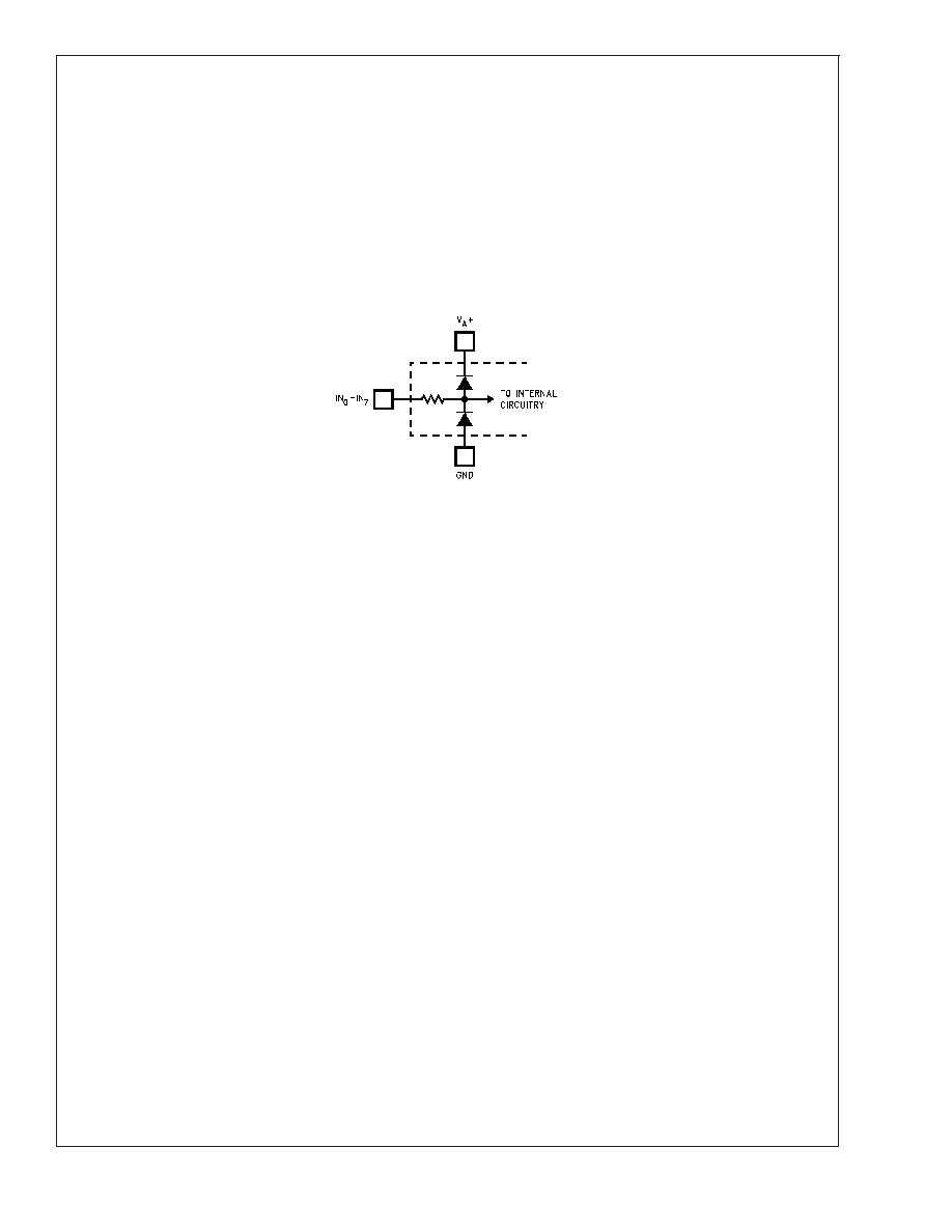
Note 6: Two on-chip diodes are tied to each analog input through a series resistor, as shown below. Input voltage magnitude up to 5V above VA+ or 5V below GND
will not damage the LM12454 or the LM12(H)458. However, errors in the A/D conversion can occur if these diodes are forward biased by more than 100 mV. As an
example, if VA+ is 4.5 VDC, full-scale input voltage must be ≤4.6 VDC to ensure accurate conversions.
01126403
Note 7: VA+ and VD+ must be connected together to the same power supply voltage and bypassed with separate capacitors at each V
+ pin to assure
conversion/comparison accuracy.
Note 8: Accuracy is guaranteed when operating at fCLK = 5 MHz for the LM12454/8 and fCLK = 8 MHz for the LM12H458.
Note 9: With the test condition for VREF (VREF+ VREF) given as +5V, the 12-bit LSB is 1.22 mV and the 8-bit/“Watchdog” LSB is 19.53 mV.
Note 10: Typical figures are at TA = 25C and represent most likely parametric norm.
Note 11: Limits are guaranteed to National’s AOQL (Average Output Quality Level).
Note 12: Positive integral linearity error is defined as the deviation of the analog value, expressed in LSBs, from the straight line that passes through positive
full-scale and zero. For negative integral linearity error the straight line passes through negative full-scale and zero. (See Figure 6 Figure 7).
Note 13: Zero error is a measure of the deviation from the mid-scale voltage (a code of zero), expressed in LSB. It is the worst-case value of the code transitions
between 1 to 0 and 0 to +1 (see Figure 8).
Note 14: The DC common-mode error is measured with both inputs shorted together and driven from 0V to 5V. The measured value is referred to the resulting
output value when the inputs are driven with a 2.5V signal.
Note 15: Power Supply Sensitivity is measured after Auto-Zero and/or Auto-Calibration cycle has been completed with VA+ and VD+ at the specified extremes.
Note 16: VREFCM (Reference Voltage Common Mode Range) is defined as (VREF+ +VREF)/2.
Note 17: The LM12(H)454/8’s self-calibration technique ensures linearity and offset errors as specified, but noise inherent in the self-calibration process will result
in a repeatability uncertainty of ±0.10 LSB.
Note 18: The Throughput Rate is for a single instruction repeated continuously. Sequencer states 0 (1 clock cycle), 1 (1 clock cycle), 7 (9 clock cycles) and 5 (44
clock cycles) are used (see Figure 15). One additional clock cycle is used to read the conversion result stored in the FIFO, for a total of 56 clock cycles per
conversion. The Throughput Rate is fCLK (MHz)/N, where N is the number of clock cycles/conversion.
LM12454/LM12458/LM12H458
www.national.com
9
相關(guān)PDF資料 |
PDF描述 |
|---|---|
| LM12458CIVF/NOPB | SPECIALTY ANALOG CIRCUIT, PQFP44 |
| LM129AGMW8 | 1-OUTPUT TWO TERM VOLTAGE REFERENCE, 6.9 V, UUC |
| LM12H458MW/883 | SPECIALTY ANALOG CIRCUIT, CQFP44 |
| 5962-9319502MXC | SPECIALTY ANALOG CIRCUIT, CQCC44 |
| LM12L454CIV | SPECIALTY ANALOG CIRCUIT, PQCC44 |
相關(guān)代理商/技術(shù)參數(shù) |
參數(shù)描述 |
|---|---|
| LM12458CIVX/NOPB | 功能描述:模數(shù)轉(zhuǎn)換器 - ADC RoHS:否 制造商:Texas Instruments 通道數(shù)量:2 結(jié)構(gòu):Sigma-Delta 轉(zhuǎn)換速率:125 SPs to 8 KSPs 分辨率:24 bit 輸入類型:Differential 信噪比:107 dB 接口類型:SPI 工作電源電壓:1.7 V to 3.6 V, 2.7 V to 5.25 V 最大工作溫度:+ 85 C 安裝風(fēng)格:SMD/SMT 封裝 / 箱體:VQFN-32 |
| LM12458CMEL/883 | 制造商:未知廠家 制造商全稱:未知廠家 功能描述:Single-Ended Data Acquisition System |
| LM12458MEL/883 | 制造商:未知廠家 制造商全稱:未知廠家 功能描述:Single-Ended Data Acquisition System |
| LM12458MW/883 | 制造商:未知廠家 制造商全稱:未知廠家 功能描述:Single-Ended Data Acquisition System |
| LM1246 | 制造商:NSC 制造商全稱:National Semiconductor 功能描述:150 MHz I2C Compatible RGB Preamplifier with Internal 512 Character OSD ROM, 512 Character RAM and 4 DACs |
發(fā)布緊急采購,3分鐘左右您將得到回復(fù)。