- 您現(xiàn)在的位置:買賣IC網(wǎng) > PDF目錄30743 > LM1238AAF/NA (NATIONAL SEMICONDUCTOR CORP) 3 CHANNEL, VIDEO PREAMPLIFIER, PDIP24 PDF資料下載
參數(shù)資料
| 型號: | LM1238AAF/NA |
| 廠商: | NATIONAL SEMICONDUCTOR CORP |
| 元件分類: | 音頻/視頻放大 |
| 英文描述: | 3 CHANNEL, VIDEO PREAMPLIFIER, PDIP24 |
| 封裝: | N24D |
| 文件頁數(shù): | 19/24頁 |
| 文件大小: | 1207K |
| 代理商: | LM1238AAF/NA |

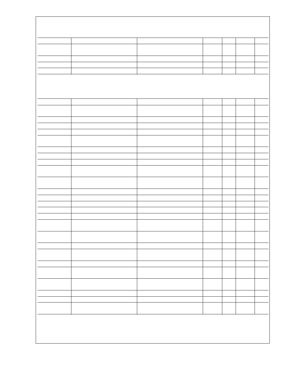
DAC Output Electrical Characteristics (Continued)
Unless otherwise noted: T
A = 25C, VCC = +5.0V, VIN = 0.7V, VABL =VCC,CL = 8 pF, Video Outputs = 2.0 VP-P. See Note 7
for Min and Max parameters and Note 6 for Typicals. DAC parameters apply to all 4 DACs.
Symbol
Parameter
Conditions
Min
Typ
Max
Units
V
Max DAC (VCC)
Variation in voltage of DAC with
V
CC
4.75 < V
CC < 5.25V
±50
mV/V
Linearity
Linearity of DAC over its range
5
%
Monotonicity
Monotonicity of the DAC
Excluding dead zones
±0.5
LSB
I
MAX
Max Load Current
1.0
mA
System Interface Signal Characteristics
Unless otherwise noted: T
A = 25C, VCC = +5.0V, VIN = 0.7V, VABL =VCC,CL = 8 pF, Video Outputs = 2.0 VP-P. See Note 7
for Min and Max parameters and Note 6 for Typicals. DAC parameters apply to all 4 DACs.
Symbol
Parameter
Conditions
Min
Typ
Max
Units
V
VTH+
VFLYBACK positive switching
guarantee.
Vertical Blanking triggered
2.0
V
SPOT
Spot Killer Voltage
Note 17, V
CC Adjusted to Activate
3.4
3.9
4.3
V
Ref
V
Ref Output Voltage
1.25
1.45
1.65
V
IL (SCL, SDA)
Logic Low Input Voltage
0.5
1.5
V
IH (SCL, SDA)
Logic High Input Voltage
3.0
V
CC +
0.5
V
I
L (SCL, SDA)
Logic Low Input Current
SDA or SCL, Input Voltage = 0.4V
±10
A
I
H (SCL, SDA)
Logic High Input Voltage
SDA or SCL, Input Voltage = 4.5V
±10
A
V
OL (SCL, SDA)
Logic Low Output Voltage
I
O = 3 mA
0.5
V
f
H Min
Minimum Horizontal Frequency
PLL & OSD Operational; PLL
Range = 0
25
kHz
f
H Max
Maximum Horizontal Frequency
PLL & OSD Operational; PLL
Range = 3
100
110
kHz
I
HFB IN Max
Horizontal Flyback Input Current
Absolute Maximum During Flyback
5
mA
I
IN
Peak Current during flyback
Design Value
4
mA
I
HFB OUT Max
Horizontal Flyback Input Current
Absolute Maximum During Scan
700
A
I
OUT
Peak Current during Scan
Design Value
550
A
I
IN THRESHOLD
I
IN H-Blank Detection Threshold
0
A
t
H-BLANK ON
H-Blank Time Delay - On
+ Zero crossing of I
HFB to 50% of
output blanking start. I
24 = +1.5mA
45
ns
t
H-BLANK OFF
H-Blank Time Delay - Off
Zero crossing of I
HFB to 50% of
output blanking end. I
24 = 100A
85
ns
V
BLANK Max
Maximum Video Blanking Level
Test Setting 4, AC input signal.
0
0.25
V
f
FREERUN
Free Run H Frequency, including H
Blank
42
kHz
t
PW CLAMP
Minimum Clamp Pulse Width
See Note 15
200
ns
V
CLAMP MAX
Maximum Low Level Clamp Pulse
Voltage
Video Clamp Functioning
2.0
V
CLAMP MIN
Minimum High Level Clamp Pulse
Voltage
Video Clamp Functioning
3.0
V
I
CLAMP Low
Clamp Gate Low Input Current
V
23 = 2V
0.4
A
I
CLAMP High
Clamp Gate High Input Current
V
23 = 3V
0.4
A
t
CLAMP-VIDEO
Time from End of Clamp Pulse to
Start of Video
Referenced to Blue, Red and Green
inputs
50
ns
Note 1: Limits of Absolute Maximum Ratings indicate below which damage to the device must not occur.
Note 2: Limits of operating ratings indicate required boundaries of conditions for which the device is functional, but may not meet specific performance limits.
Note 3: All voltages are measured with respect to GND, unless otherwise specified.
Note 4: Human body model, 100 pF discharged through a 1.5 k
resistor.
LM1238
www.national.com
4
相關(guān)PDF資料 |
PDF描述 |
|---|---|
| LM1246AAA/NA | 3 CHANNEL, VIDEO PREAMPLIFIER, PDIP24 |
| LM1247AAG/NA/NOPB | 3 CHANNEL, VIDEO PREAMPLIFIER, PDIP24 |
| LM1253AAE/NA | ON-SCREEN DISPLAY IC, PDIP28 |
| LM1267NA/NOPB | 3 CHANNEL, VIDEO PREAMPLIFIER, PDIP24 |
| LM1269NA/NOPB | 3 CHANNEL, VIDEO PREAMPLIFIER, PDIP24 |
相關(guān)代理商/技術(shù)參數(shù) |
參數(shù)描述 |
|---|---|
| LM123AK-05 | 制造商:未知廠家 制造商全稱:未知廠家 功能描述:Voltage Regulator |
| LM123AK-05-883B | 制造商:未知廠家 制造商全稱:未知廠家 功能描述:Voltage Regulator |
| LM123AK-12 | 制造商:未知廠家 制造商全稱:未知廠家 功能描述:Voltage Regulator |
| LM123AK-12-883B | 制造商:未知廠家 制造商全稱:未知廠家 功能描述:Voltage Regulator |
| LM123AK-15 | 制造商:未知廠家 制造商全稱:未知廠家 功能描述:Voltage Regulator |
發(fā)布緊急采購,3分鐘左右您將得到回復(fù)。