- 您現(xiàn)在的位置:買賣IC網(wǎng) > PDF目錄358775 > LD502PLID Analog IC PDF資料下載
參數(shù)資料
| 型號(hào): | LD502PLID |
| 英文描述: | Analog IC |
| 中文描述: | 模擬IC |
| 文件頁數(shù): | 4/4頁 |
| 文件大?。?/td> | 159K |
| 代理商: | LD502PLID |
4
500 - 43 - 18
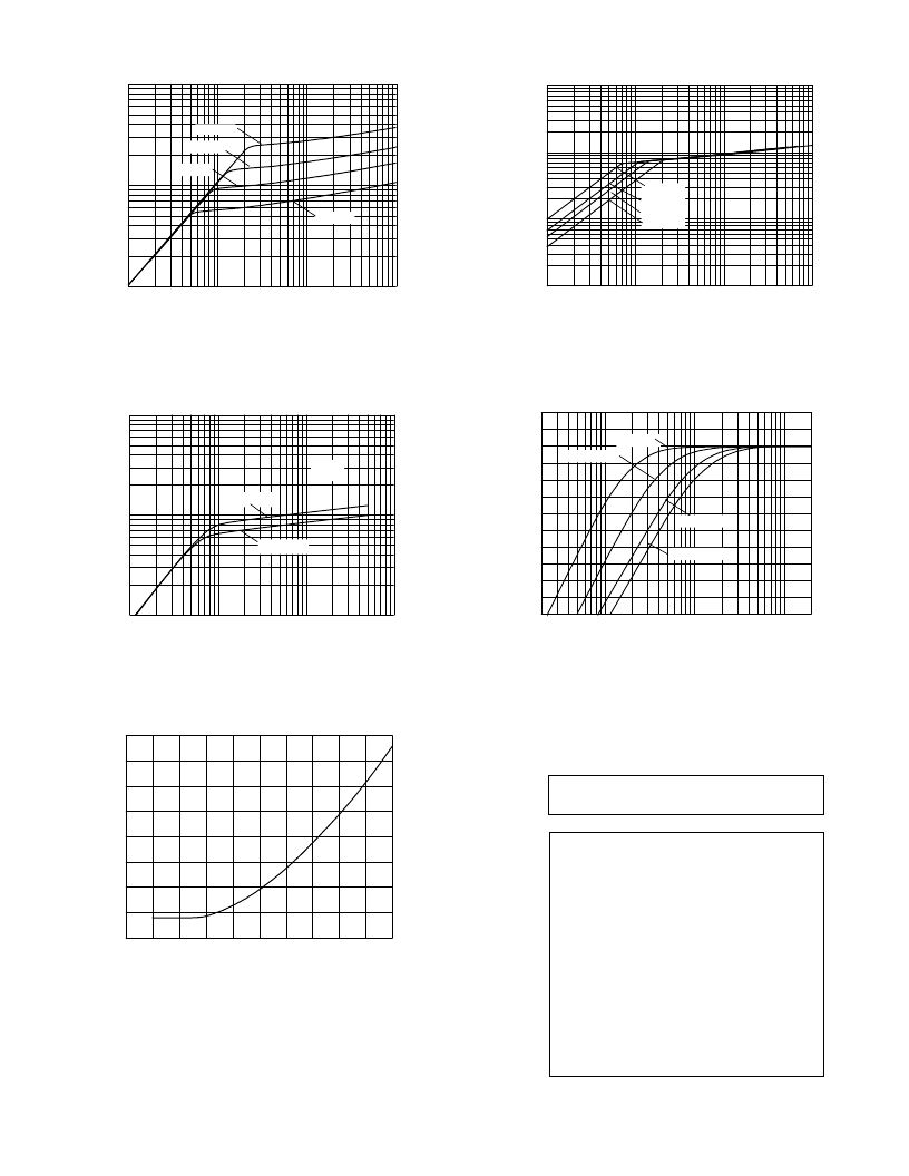
Fig. 8 Total Harmonic Distortion
vs Output Level
4.0
3.0
2.0
1.0
0.0
0.0
5.0
10.0
15.0
20.0
25.0
OUTPUT (mV)
T
100
0.01
0.1
1.0
10
INPUT (mV)
Fig. 5 I/O Characteristics at
Various R
GT
Values
0.1
1
10
R
GT
=130k
R
GT
=82k
R
GT
=68k
R
GT
=47k
100
0.01
0.1
1.0
10
INPUT (mV)
Fig. 6 Effects of Supply Voltage
Variation
0.1
10
V
B
=3 VDC
V
B
=1.3 VDC
Fig. 7 Frequency Response at
Various C
S
Values
O
100
10
1
0.01
0.1
1.0
10
INPUT (mV)
Fig. 4 I/O Characteristics at
Various R
TH
Values
R
TH
=0k
R
TH
=10k
R
TH
=22k
R
TH
=50k
4
2
0
-2
-4
-6
-8
-10
-12
-14
-16
-18
-20
C
S
=0.1
μ
C
S
=0.22
μ
C
S
=0.047
μ
C
S
=0.033
μ
20 200 2K
20000
FREQUENCY (Hz)
R
O
O
R
TH
=0
Gennum Corporation assumes no responsibility for the use of any circuits described herein and makes no representations that they are free from patent infringement.
Copyright January 1982 Gennum Corporation. All rights reserved. Printed in Canada.
DOCUMENT
IDENTIFICATION
PRODUCT PROPOSAL
This data has been compiled for market investigation purposes
only, and does not constitute an offer for sale.
ADVANCE INFORMATION NOTE
This product is in development phase and specifications are
subject to change without notice. Gennum reserves the right to
remove the product at any time. Listing the product does not
constitute an offer for sale.
PRELIMINARY DATA SHEET
The product is in a preproduction phase and specifications are
subject to change without notice.
DATA SHEET
The product is in production. Gennum reserves the right to make
changes at any time to improve reliability, function or design, in
order to provide the best product possible.
REVISION NOTES
Changes to Fig.1, test conditions, Pb/Sn bump removed.
相關(guān)PDF資料 |
PDF描述 |
|---|---|
| LD502MINI | Analog IC |
| LD502MCRO | Analog IC |
| LD505 | High Gain Class A Amplifier |
| LD549 | High Power Class B Output Stage |
| LD646A | 16-BIT BUS TRANSCEIVER AND REGISTER WITH 3-STATE OUTPUTS |
相關(guān)代理商/技術(shù)參數(shù) |
參數(shù)描述 |
|---|---|
| LD502SLT | 制造商:未知廠家 制造商全稱:未知廠家 功能描述:Analog IC |
| LD5033MDL | 制造商:Opnext 功能描述:LASER, PBX, XLCIA, L0 (-4.0,-0.1) - Bulk |
| LD5035SMDL | 制造商:Opnext 功能描述:LASER, PBX, XLCIA, L0 (-4.0,-0.1) - Bulk |
| LD5035SMDL-W | 制造商:Opnext 功能描述:LASER, PBX, XLCIA, L0 (-4.0,-0.1) - Bulk |
| LD5038SMDL | 制造商:Opnext 功能描述:TRANSEIVER - Bulk |
發(fā)布緊急采購,3分鐘左右您將得到回復(fù)。