- 您現(xiàn)在的位置:買賣IC網 > PDF目錄358771 > LC895925 (Sanyo Electric Co.,Ltd.) Signal Processing LSI for CD-R Drives PDF資料下載
參數資料
| 型號: | LC895925 |
| 廠商: | Sanyo Electric Co.,Ltd. |
| 英文描述: | Signal Processing LSI for CD-R Drives |
| 中文描述: | 信號處理LSI的CD - R驅動器 |
| 文件頁數: | 7/7頁 |
| 文件大小: | 90K |
| 代理商: | LC895925 |
PS No. 5784-7/7
LC895925
This catalog provides information as of December, 1997. Specifications and information herein are subject to
change without notice.
I
No products described or contained herein are intended for use in surgical implants, life-support systems, aerospace
equipment, nuclear power control systems, vehicles, disaster/crime-prevention equipment and the like, the failure of
which may directly or indirectly cause injury, death or property loss.
I
Anyone purchasing any products described or contained herein for an above-mentioned use shall:
Accept full responsibility and indemnify and defend SANYO ELECTRIC CO., LTD., its affiliates, subsidiaries and
distributors and all their officers and employees, jointly and severally, against any and all claims and litigation and all
damages, cost and expenses associated with such use:
Not impose any responsibility for any fault or negligence which may be cited in any such claim or litigation on
SANYO ELECTRIC CO., LTD., its affiliates, subsidiaries and distributors or any of their officers and employees
jointly or severally.
I
Information (including circuit diagrams and circuit parameters) herein is for example only; it is not guaranteed for
volume production. SANYO believes information herein is accurate and reliable, but no guarantees are made or implied
regarding its use or any infringements of intellectual property rights or other rights of third parties.
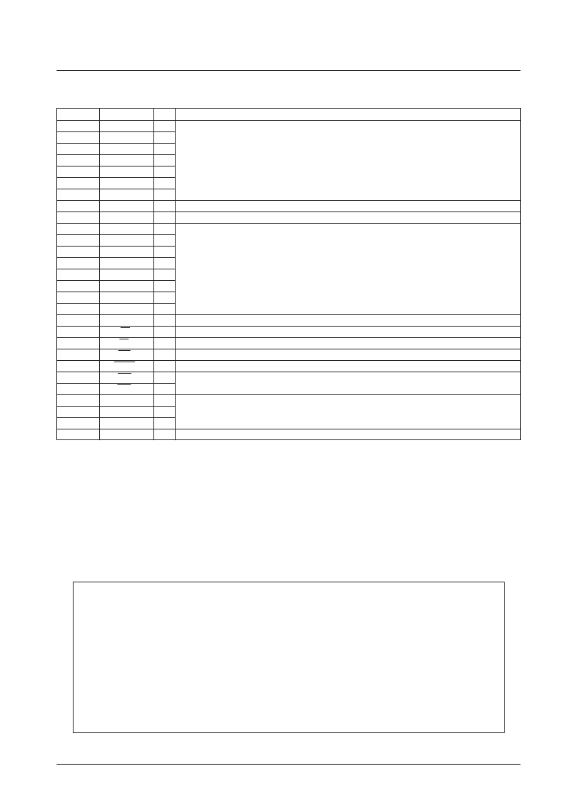
Continued from preceding page.
Type: I: Input pin, O: Output pin, B: Bidirectional pin, P: Power supply pin, N: No connection pin
Pin Number
Pin Name
Type
Description
133
SUA0
I
134
SUA1
I
135
SUA2
I
136
SUA3
I
Command register selection address input pinsI
137
SUA4
I
138
SUA5
I
139
SUA6
I
140
V
DD
V
SS
D0
P
141
P
142
B
143
D1
B
144
D2
B
145
D3
B
146
D4
B
Microcontroller data signal pins, with pull-up resistors
147
D5
B
148
D6
B
149
D7
B
150
V
DD
CS
P
151
I
Chip select signal from microcontroller
152
RD
I
Data read signal from microcontroller
153
WR
I
Data write signal from microcontroller
154
SWAIT
O
Wait signal to microcontroller
155
INT0
O
Interrupt request signals to microcontroller. Open drain outputs with built-in pull-up resistors
156
INT1
O
157
Reserve3
B
158
Reserve4
B
Reserved for future expansion (leave open)
159
Reserve5
B
160
V
DD
P
相關PDF資料 |
PDF描述 |
|---|---|
| LC895926 | CD-R Encoder/Decoder IC with Built-in SCSI Interface |
| LC895994 | CD-R Encoder/Decoder LSI with Built-in ATAPI (IDE) Interface |
| LC89602 | Audio Decoder LSI for Mini-Disk Playback(用于微型磁盤回放的音頻譯碼器LSI) |
| LC89610 | Mini-Disk Decoder LSI |
| LC897127K | SCSI CD-ROM Decoder with On-Chip DVD Interface |
相關代理商/技術參數 |
參數描述 |
|---|---|
| LC895926 | 制造商:SANYO 制造商全稱:Sanyo Semicon Device 功能描述:CD-R Encoder/Decoder IC with Built-in SCSI Interface |
| LC895994 | 制造商:SANYO 制造商全稱:Sanyo Semicon Device 功能描述:CD-R Encoder/Decoder LSI with Built-in ATAPI (IDE) Interface |
| LC89602 | 制造商:SANYO 制造商全稱:Sanyo Semicon Device 功能描述:Audio Decoder LSI for Mini-Disk Playback |
| LC89610 | 制造商:SANYO 制造商全稱:Sanyo Semicon Device 功能描述:Mini-Disk Decoder LSI |
| LC896431 | 制造商:未知廠家 制造商全稱:未知廠家 功能描述: |
發(fā)布緊急采購,3分鐘左右您將得到回復。