- 您現(xiàn)在的位置:買賣IC網(wǎng) > PDF目錄358761 > LC7444 (Sanyo Electric Co.,Ltd.) Dual VCO(Voltage Controlled Oscillator)Circuit(雙電壓控制振蕩器電路) PDF資料下載
參數(shù)資料
| 型號(hào): | LC7444 |
| 廠商: | Sanyo Electric Co.,Ltd. |
| 英文描述: | Dual VCO(Voltage Controlled Oscillator)Circuit(雙電壓控制振蕩器電路) |
| 中文描述: | 雙VCO(壓控振蕩器)電路(雙電壓控制振蕩器電路) |
| 文件頁(yè)數(shù): | 3/3頁(yè) |
| 文件大小: | 42K |
| 代理商: | LC7444 |
PS No. 4305-3/3
LC7444
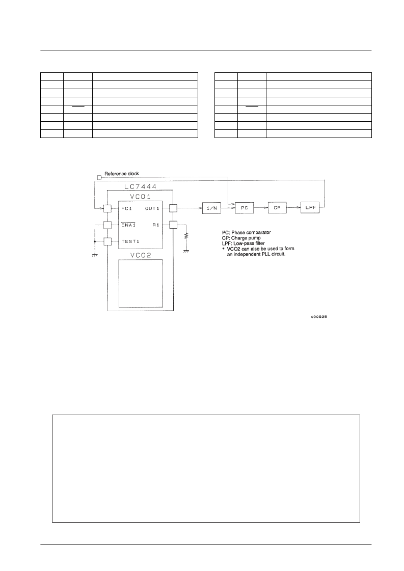
Pin Functions
Sample Application
Pin No.
Symbol
Function
1
V
DD
1
OUT1
Power supply
2
VCO1 clock output
3
TEST1
Test pin. Must be tied low in normal operation.
4
ENA1
VCO1 enable input
5
R1
VCO1 oscillator range resistor
6
FC1
VCO1 control voltage input
7
V
SS
1
Ground
Pin No.
Symbol
Function
8
V
SS
2
FC2
Ground
9
VCO2 control voltage input
10
R2
VCO2 oscillator range resistor
11
ENA2
VCO2 enable input
12
TEST2
Test pin
13
OUT2
VCO2 clock output
14
V
DD
2
Power supply
This catalog provides information as of May, 1995. Specifications and information herein are subject to change
without notice.
I
No products described or contained herein are intended for use in surgical implants, life-support systems, aerospace
equipment, nuclear power control systems, vehicles, disaster/crime-prevention equipment and the like, the failure of
which may directly or indirectly cause injury, death or property loss.
I
Anyone purchasing any products described or contained herein for an above-mentioned use shall:
Accept full responsibility and indemnify and defend SANYO ELECTRIC CO., LTD., its affiliates, subsidiaries and
distributors and all their officers and employees, jointly and severally, against any and all claims and litigation and all
damages, cost and expenses associated with such use:
Not impose any responsibility for any fault or negligence which may be cited in any such claim or litigation on
SANYO ELECTRIC CO., LTD., its affiliates, subsidiaries and distributors or any of their officers and employees
jointly or severally.
I
Information (including circuit diagrams and circuit parameters) herein is for example only; it is not guaranteed for
volume production. SANYO believes information herein is accurate and reliable, but no guarantees are made or implied
regarding its use or any infringements of intellectual property rights or other rights of third parties.
相關(guān)PDF資料 |
PDF描述 |
|---|---|
| LC7454A | CMOS Data Slicer(CMOS 數(shù)據(jù)切波器) |
| LC7455A | Closed Caption Signal Extraction IC(從重疊視頻信號(hào)中提取接近字符信號(hào)的芯片) |
| LC7455 | Closed Caption Signal Extraction IC |
| LC7456A | U.S. Closed Caption Signal Extraction IC |
| LC7458B-04 | Closed-Caption Decoder LSI |
相關(guān)代理商/技術(shù)參數(shù) |
參數(shù)描述 |
|---|---|
| LC744E | 制造商:Brady Corporation 功能描述:PRINZING SMALL YELLOW LOCKOUT BOARD |
| LC7450 | 制造商:未知廠家 制造商全稱:未知廠家 功能描述: |
| LC7450H | 制造商:未知廠家 制造商全稱:未知廠家 功能描述:Analog IC |
| LC7450M | 制造商:未知廠家 制造商全稱:未知廠家 功能描述:Analog IC |
| LC7450N | 制造商:未知廠家 制造商全稱:未知廠家 功能描述:Analog IC |
發(fā)布緊急采購(gòu),3分鐘左右您將得到回復(fù)。