- 您現(xiàn)在的位置:買賣IC網(wǎng) > PDF目錄358759 > LC72341G (Sanyo Electric Co.,Ltd.) Low-Voltage Single-Chip Microcontrollers with On-Chip PLL and LCD Driver Circuits(用于音頻設(shè)備的低電壓單片微控制器(帶片上鎖相環(huán)電路和LCD驅(qū)動器)) PDF資料下載
參數(shù)資料
| 型號: | LC72341G |
| 廠商: | Sanyo Electric Co.,Ltd. |
| 英文描述: | Low-Voltage Single-Chip Microcontrollers with On-Chip PLL and LCD Driver Circuits(用于音頻設(shè)備的低電壓單片微控制器(帶片上鎖相環(huán)電路和LCD驅(qū)動器)) |
| 中文描述: | 低電壓的單芯片微控制器芯片PLL和LCD驅(qū)動電路(用于音頻設(shè)備的低電壓單片微控制器(帶片上鎖相環(huán)電路和液晶顯示驅(qū)動器)) |
| 文件頁數(shù): | 7/12頁 |
| 文件大小: | 171K |
| 代理商: | LC72341G |
No. 5799-7/12
LC72341G/W, 72342G/W, 72343G/W
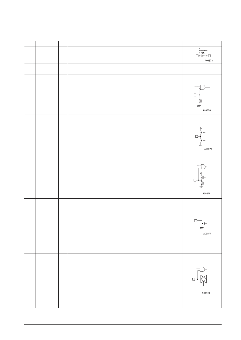
Pin Functions
Pin No.
Pin
I/O
Function
I/O circuit
64
1
XIN
XOUT
I
O
Connections for a 75-kHz crystal oscillator element
63
2
TEST1
TEST2
I
I
IC test pins. These pins must be tied to ground.
Input with built-in pull-
down resistor
6
5
4
3
PA0
PA1
PA2
PA3
I
Special-purpose key return signal input ports designed with a low threshold voltage.
When used in conjunction with port PB to form a key matrix, up to 3 simultaneous key
presses can be detected. The four pull-down resistors are selected together in a single
operation using the IOS instruction (PWn = 2, b1); they cannot be specified individually.
Input is disabled in backup mode, and the pull-down resistors are disabled after a reset.
Unbalanced CMOS
push-pull circuit
10
9
8
7
PB3
PB2
PB1
PB0
O
Special-purpose key source signal output ports. Since unbalanced CMOS output
transistor circuits are used, diodes to prevent short-circuits when multiple keys are
pressed are not required. These ports go to the output high-impedance state in backup
mode. These ports go to the output high-impedance state after a reset and remain in that
state until an output instruction (OUT, SPB, or RPB) is executed.
Care is required in designing the output loads if these pins are used for functions other
than key source outputs.
CMOS push-pull circuit
14
13
12
11
18
17
16
15
PC0
PC1
PC2
PC3
INT/PD0
PD1
PD2
PD3
I/O
General-purpose I/O ports
*.
PD0 can be used as an external interrupt port. Input or
output mode can be set in a bit unit using the IOS instruction (Pwn = 4, 5). A value of 0
specifies input, and 1 specifies output. These ports go to the input disabled high-
impedance state in backup mode. They are set to function as general-purpose input ports
after a reset.
N-channel open drain
20
19
BEEP/PE0
PE1
General-purpose output ports with shared beep tone output function (PE0 only). The
BEEP instruction is used to switch PE0 between the general-purpose output port and
beep tone output functions. To use PE0 as a general-purpose output port, execute a
BEEP instruction with b2 set to 0. Set b2 to 1 to use PE0 as the beep tone output port.
The b0 and b1 bits are used to select the beep tone frequency. There are two beep tone
frequencies supported.
When PE0 is set up as the beep tone output, executing an output instruction to PN0 only
changes the state of the internal output latch, it does not affect the beep tone output in
any way. Only the PE0 pin can be switched between the general-purpose output
function and the beep tone output function; the PE1 pin only functions as a general-
purpose output. These pins go to the high-impedance state in backup mode and remain
in that state until an output instruction or a BEEP instruction is executed. Since these
ports are open-drain ports, resistors must be inserted between these pins and V
DD
.
These ports are set to their general-purpose output port function after a reset.
CMOS input/analog
input
23
22
21
PF0/ADI0
PF1/ADI1
PF2
I
General-purpose input and A/D converter input shared function ports (PF2 is a general-
purpose input only port). The IOS instruction (Pwn = FH) is used to switch between the
general-purpose input and A/D converter port functions. The general-purpose input and
A/D converter port functions can be switched in a bit unit, with 0 specifying general-
purpose input, and 1 specifying the A/D converter input function. To select the A/D
converter function, set up the A/D converter pin with an IOS instruction with Pwn set to 1.
The A/D converter is started with the UCC instruction (b3 = 1, b2 = 1). The ADCE flag is
set when the conversion completes. The INR instruction is used to read in the data.
If an input instruction is executed for one of these pins which is set up for analog input,
the read in data will be at the low level since CMOS input is disabled. In backup mode
these pins go to the input disabled high-impedance state. These ports are set to their
general-purpose input port function after a reset. The A/D converter is a 5-bit successive
approximation type converter, and features a conversion time of 1.28 ms. Note that the
full-scale A/D converter voltage (1FH) is (63 · 96)V
DD
.
Continued on next page.
Note:
*
Applications must establish the output data in advance with an OUT, SPB, or RPB instruction and then set the pin to output mode with an IOS
instruction when using the I/O switchable ports as output pins.
相關(guān)PDF資料 |
PDF描述 |
|---|---|
| LC72345 | Low-Voltage ETR Controller with On-Chip DC-DC Converter |
| LC72346 | Ultralow-Voltage ETR Controller with On-Chip LCD Driver |
| LC72346W | Ultralow-Voltage ETR Controller with On-Chip LCD Driver |
| LC72349 | Low-Voltage ETR Controller with On-Chip LCD Driver |
| LC72349W | Low-Voltage ETR Controller with On-Chip LCD Driver |
相關(guān)代理商/技術(shù)參數(shù) |
參數(shù)描述 |
|---|---|
| LC72341W | 制造商:SANYO 制造商全稱:Sanyo Semicon Device 功能描述:Low-Voltage Single-Chip Microcontrollers with On- Chip PLL and LCD Driver Circuits |
| LC72342G | 制造商:SANYO 制造商全稱:Sanyo Semicon Device 功能描述:Low-Voltage Single-Chip Microcontrollers with On- Chip PLL and LCD Driver Circuits |
| LC72342W | 制造商:SANYO 制造商全稱:Sanyo Semicon Device 功能描述:Low-Voltage Single-Chip Microcontrollers with On- Chip PLL and LCD Driver Circuits |
| LC72342-XXXX | 制造商:未知廠家 制造商全稱:未知廠家 功能描述: |
| LC72343G | 制造商:SANYO 制造商全稱:Sanyo Semicon Device 功能描述:Low-Voltage Single-Chip Microcontrollers with On- Chip PLL and LCD Driver Circuits |
發(fā)布緊急采購,3分鐘左右您將得到回復(fù)。