- 您現(xiàn)在的位置:買賣IC網(wǎng) > PDF目錄43903 > LC72146V PLL FREQUENCY SYNTHESIZER, 40 MHz, PDSO24 PDF資料下載
參數(shù)資料
| 型號: | LC72146V |
| 元件分類: | PLL合成/DDS/VCOs |
| 英文描述: | PLL FREQUENCY SYNTHESIZER, 40 MHz, PDSO24 |
| 封裝: | SSOP-24 |
| 文件頁數(shù): | 7/22頁 |
| 文件大?。?/td> | 157K |
| 代理商: | LC72146V |
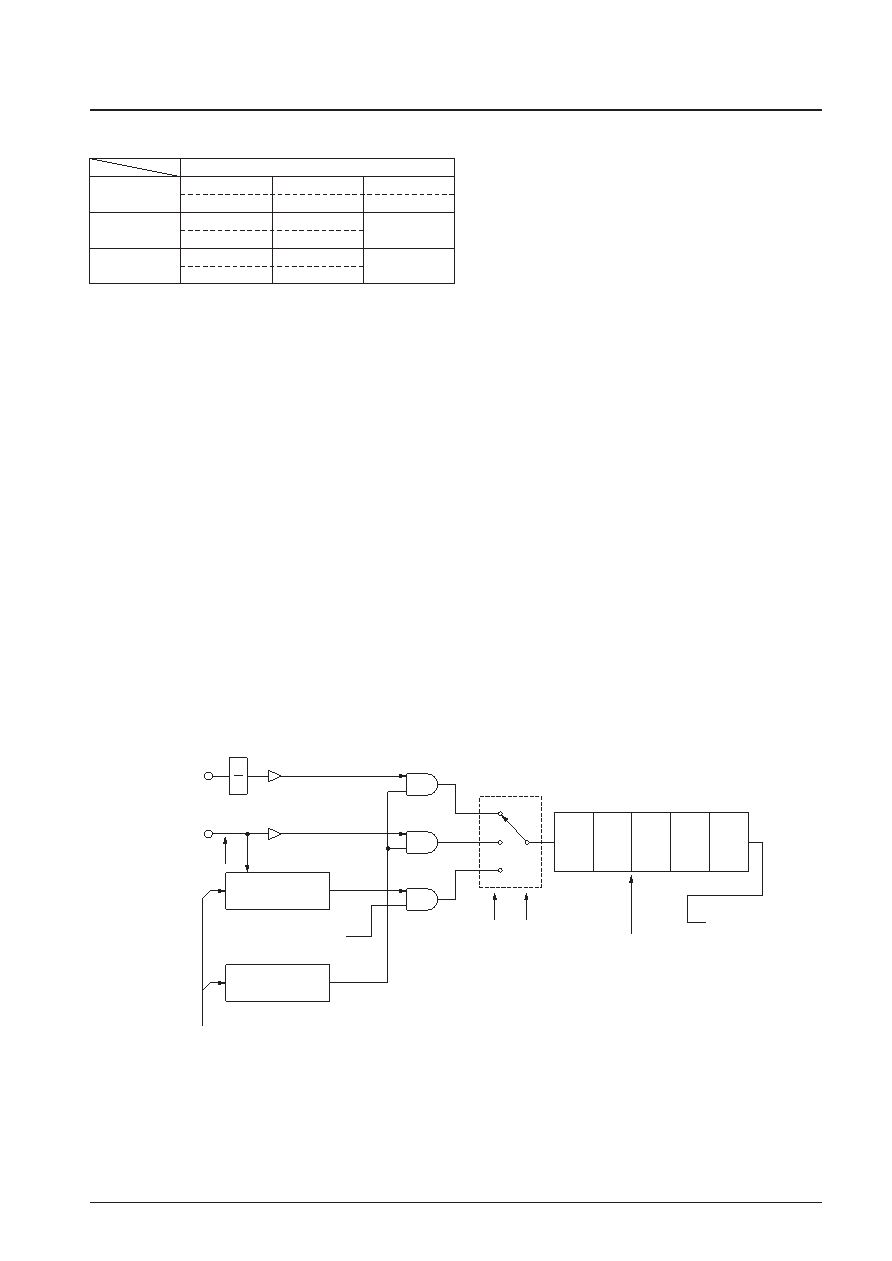
Table 15 Input Sensitivity (Target Sensitivity)
CTC: Input sensitivity switching data. When CTC is 1 the input sensitivity is degraded.However, the actual values will be:
HCTR
→ 30 to 40 mVrms (frequency: 10.7 MHz)
LCTR
→ 10 to 15 mVrms (frequency: 450 kHz)
CTP: The input pull-down resistor (when CTE is 0) can be disabled by setting CTP to 1.
CTP must be set to 1 at least 4 ms before CTE is set to 1. CTP should be set to 0 if the counter is not used.
When CTP is set to 1 wait time is reduced at 1 to 2 ms.
The LC72146 includes a general-purpose 20-bit binary counter whose value can be read out from the DO pin, MBS first.
When using this counter for frequency measurement, one of four measurement times (4, 8, 32, or 64 ms) is selected by
GT0 and GT1. The frequency input to either the HCTR or the LCTR pin can be measured by determining the number of
pulses input to the counter during the measurement period.
This counter can be used to measure the period of the signal input to the LCTR pin by determining how many cycles of a
reference signal (900 kHz) are input to the counter during one or two periods of the LCTR pin signal.
The counter is started by setting the serial data CTE bit to 1. While serial data is latched in the LC72146 when CE falls
from high to low, input to the HCTR or the LCTR pin must be provided within the waiting period that follows CE being
set low.
Next, after the measurement completes, the value of the counter must be read out during the period that CTE is 1. (The
general-purpose counter is reset when CTE is set to 0.)
It should be emphasized here that the counter should be reset before measurement by setting CTE to 0.
Also note that although the signal input to the LCTR pin is input to the counter directly, the signal input to the HCTR pin
is divided by two internally before being input to the counter. Accordingly, the value of the counter will be 1/2 the actual
frequency input to the HCTR pin.
Figure 8 General-Purpose Counter
No. 4922-15/22
LC72146, 72146M, 72146V
Minimum input sensitivity (f [MHz])
(A) FMIN
10
≤ f < 50
50
≤ f < 130
130
≤ f < 160
70 mVrms
40 mVrms
70 mVrms
(B) AMIN
2
≤ f < 25
25
≤ f < 40
—
40 mVrms
70 mVrms
(C) AMIN
0.5
≤ f < 2.5
2.5
≤ f < 10
—
40 mVrms
70 mVrms
General-purpose counter
(20-bit binary counter)
DO pin
Input signal
switching gate
S1
L
S
B
M
S
B
0 to 3
4 to 7
8 to 11 12 to 1516 to 19
S2
S3
HCTR
LCTR
(FIF)
GT1,GT0
(T)
CTC, CTP
CTS1 CTS0
CTE
C = FIF
× GT
C = (1/T)
÷ 900kHz
GT
Check signal: 900 kHz
One period/two period
extraction circuit
4/8/32/64
ms
1
2
相關(guān)PDF資料 |
PDF描述 |
|---|---|
| LC72146M | PLL FREQUENCY SYNTHESIZER, 40 MHz, PDSO24 |
| LC72147V | PLL FREQUENCY SYNTHESIZER, 180 MHz, PDSO24 |
| LC72148V | PLL FREQUENCY SYNTHESIZER, 40 MHz, PDSO24 |
| LC72191M | PLL FREQUENCY SYNTHESIZER, 40 MHz, PDSO24 |
| LC7730M | PULSE; RECTANGULAR, TIMER, PDSO16 |
相關(guān)代理商/技術(shù)參數(shù) |
參數(shù)描述 |
|---|---|
| LC72147V | 制造商:SANYO 制造商全稱:Sanyo Semicon Device 功能描述:PLL Frequency Synthesizer for Electronic Tuning in Car Audio Systems |
| LC72148V | 制造商:SANYO 制造商全稱:Sanyo Semicon Device 功能描述:Electronic Tuning PLL Frequency Synthesizer for Car Stereo Systems |
| LC72148V-MPB-E | 制造商:ON Semiconductor 功能描述:PLL FREQUENCY SYNTHESIZER - Ammo Pack 制造商:ON Semiconductor 功能描述:Phase Locked Loops - PLL |
| LC72148V-TLM-E | 功能描述:時鐘合成器/抖動清除器 RoHS:否 制造商:Skyworks Solutions, Inc. 輸出端數(shù)量: 輸出電平: 最大輸出頻率: 輸入電平: 最大輸入頻率:6.1 GHz 電源電壓-最大:3.3 V 電源電壓-最小:2.7 V 封裝 / 箱體:TSSOP-28 封裝:Reel |
| LC7215 | 制造商:SANYO 制造商全稱:Sanyo Semicon Device 功能描述:MW/LW PLL Frequency Synthesizers |
發(fā)布緊急采購,3分鐘左右您將得到回復(fù)。