- 您現(xiàn)在的位置:買賣IC網(wǎng) > PDF目錄358757 > LC662308A (Sanyo Electric Co.,Ltd.) Four-Bit Single-Chip Microcontroller with 16 KB of On-Chip OTP PROM PDF資料下載
參數(shù)資料
| 型號(hào): | LC662308A |
| 廠商: | Sanyo Electric Co.,Ltd. |
| 英文描述: | Four-Bit Single-Chip Microcontroller with 16 KB of On-Chip OTP PROM |
| 中文描述: | 四位單片機(jī)與16 KB的片上微控制器檢察官辦公室胎膜早破 |
| 文件頁數(shù): | 17/28頁 |
| 文件大小: | 205K |
| 代理商: | LC662308A |
第1頁第2頁第3頁第4頁第5頁第6頁第7頁第8頁第9頁第10頁第11頁第12頁第13頁第14頁第15頁第16頁當(dāng)前第17頁第18頁第19頁第20頁第21頁第22頁第23頁第24頁第25頁第26頁第27頁第28頁
Continued from preceding page.
Note: 1. With the output Nch transistor off in shared I/O ports with the open-drain output specifications. These pins cannot be used as input pins if the
CMOS output specifications are selected.When the port option is selected for PE.
2. With the output Nch transistor off in shared I/O ports with the open-drain output specifications. The rating for the pull-up output specification pins is
stipulated in terms of the output pull-up current IPO. These pins cannot be used as input pins if the CMOS output specifications are selected.
3. With the output Nch transistor off for CMOS output specification pins. (Also applies when the Pch open-drain option is selected for P8.)
4. With the output Nch transistor off for pull-up output specification pins.
5. When CMOS output specifications are selected for P8.
6. With the output Nch transistor off for open-drain output specification pins.
7. With the output Pch transistor off for open-drain output specification pins.
8. Reset state
Comparator Characteristics
at Ta = –30 to +70°C, V
SS
= 0 V
Note: 1. Does not include the quantization error.
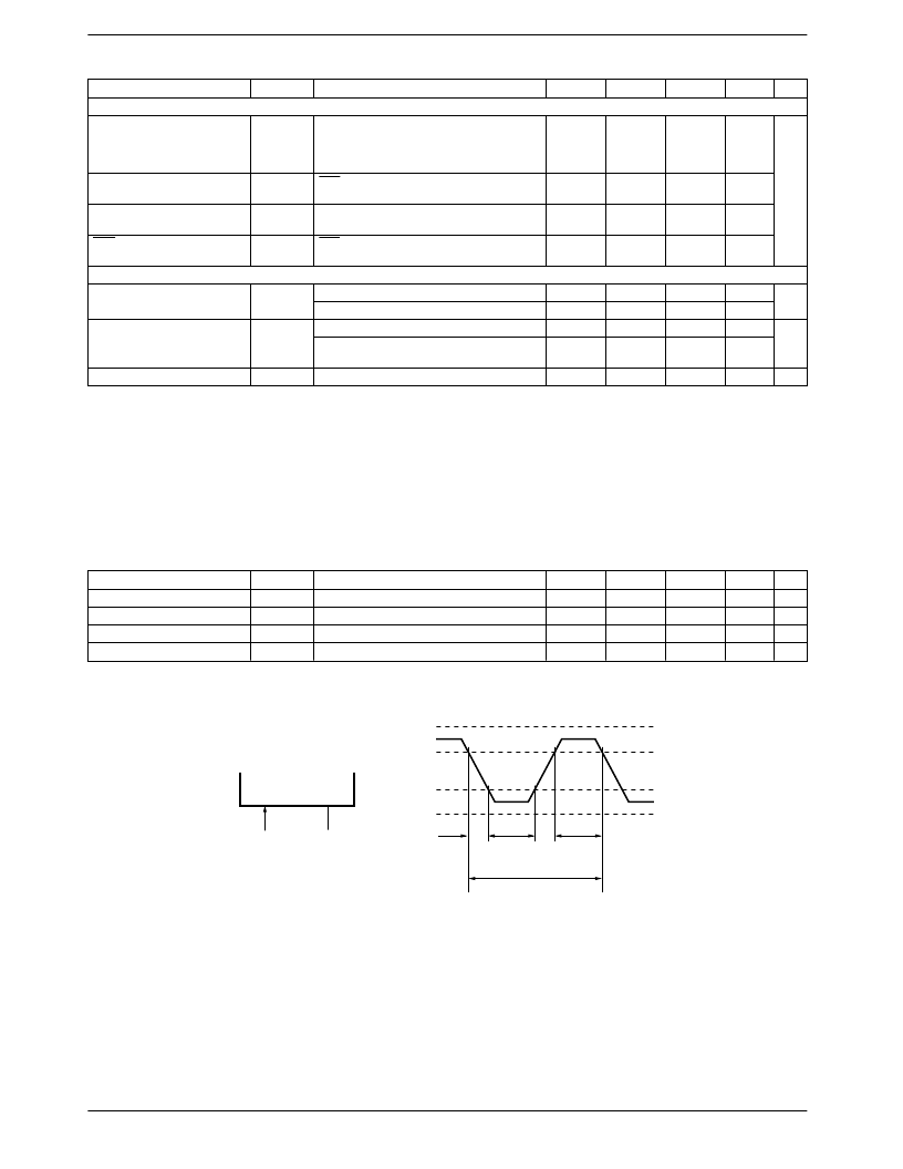
Figure 1 External Clock Input Waveform
No. 5489-17/28
LC66P5316
Parameter
Symbol
Conditions
min
typ
max
Unit
Note
[Pulse conditions]
INT0: Figure 6, conditions under which the INT0
interrupt can be accepted, conditions under
which the timer 0 event counter or pulse width
measurement input can be accepted
INT0 high and low-level
t
IOH
, t
IOL
2
Tcyc
High and low-level pulse widths
for interrupt inputs other than INT0
t
IIH
, t
IIL
INT1, INT2: Figure 6, conditions under which
the corresponding interrupt can be accepted
2
Tcyc
PIN1 high and low-level
pulse widths
t
PINH
, t
PINL
PIN1: Figure 6, conditions under which the
timer 1 event counter input can be accepted
2
Tcyc
RES high and low-level
pulse widths
t
RSH
, t
RSL
RES: Figure 6, conditions under which reset
can be applied.
3
Tcyc
Operating current drain
I
DD OP
V
DD
: 4-MHz ceramic oscillator
V
DD
: 4-MHz external clock
V
DD
: 4-MHz ceramic clock
V
DD
: 32 kHz (main oscillator stopped),
sub-oscillator: crystal
6.0
12
mA
8
6.0
12
mA
4.0
8
mA
Halt mode current drain
I
DDHALT
100
500
μA
Hold mode current drain
I
DDHOLD
V
DD
: V
DD
= 1.8 to 5.5 V
0.01
10
μA
Parameter
Symbol
Conditions
min
typ
max
Unit
Note
Absolute precision
V
CECM
V
THCM
V
INCM
T
CCM
AN1 to AN4: V
DD
= 4.0 to 5.5 V
V
DD
= 4.0 to 5.5 V
AN1 to AN4: V
DD
= 4.0 to 5.5 V
V
DD
= 4.0 to 5.5 V
±1/2
±1
LSB
1
Threshold voltage
V
SS
V
SS
V
DD
V
DD
30
V
Input voltage
V
Conversion time
μs
textL
OPEN
(OSC2)
OSC1
textR
1/fext
textF
VSS
VDD
0.2VDD
0.8VDD
textH
External clock
相關(guān)PDF資料 |
PDF描述 |
|---|---|
| LC662508A | Four-Bit Single-Chip Microcontrollers with 8, 12, and 16 KB of On-Chip ROM |
| LC66306A | 6K-Byte ROM-Contained Single-Chip 4-Bit Microcontroller for Control-Oriented Application(用于控制導(dǎo)向的單片4位微控制器(帶6K字節(jié)ROM)) |
| LC66354A | Hex Inverters 14-PDIP -40 to 85 |
| LC66354B | Quadruple 2-Input Positive-AND Gates 14-SO -40 to 85 |
| LC66354C | Quadruple 2-Input Positive-AND Gates 14-TSSOP -40 to 85 |
相關(guān)代理商/技術(shù)參數(shù) |
參數(shù)描述 |
|---|---|
| LC662312A | 制造商:SANYO 制造商全稱:Sanyo Semicon Device 功能描述:Four-Bit Single-Chip Microcontroller with 16 KB of On-Chip OTP PROM |
| LC662316A | 制造商:SANYO 制造商全稱:Sanyo Semicon Device 功能描述:Four-Bit Single-Chip Microcontroller with 16 KB of On-Chip OTP PROM |
| LC662508A | 制造商:SANYO 制造商全稱:Sanyo Semicon Device 功能描述:Four-Bit Single-Chip Microcontroller with 16 KB of On-Chip OTP PROM |
| LC662508A(DIP64) | 制造商:未知廠家 制造商全稱:未知廠家 功能描述:4-Bit Microcontroller |
| LC662508A(QFP64) | 制造商:未知廠家 制造商全稱:未知廠家 功能描述:4-Bit Microcontroller |
發(fā)布緊急采購,3分鐘左右您將得到回復(fù)。