- 您現(xiàn)在的位置:買賣IC網(wǎng) > PDF目錄358757 > LC65E43 (Sanyo Electric Co.,Ltd.) One-Time Programmable 4-Bit Single-Chip Microcontroller PDF資料下載
參數(shù)資料
| 型號: | LC65E43 |
| 廠商: | Sanyo Electric Co.,Ltd. |
| 英文描述: | One-Time Programmable 4-Bit Single-Chip Microcontroller |
| 中文描述: | 一次性可編程4位單片機 |
| 文件頁數(shù): | 10/14頁 |
| 文件大小: | 261K |
| 代理商: | LC65E43 |
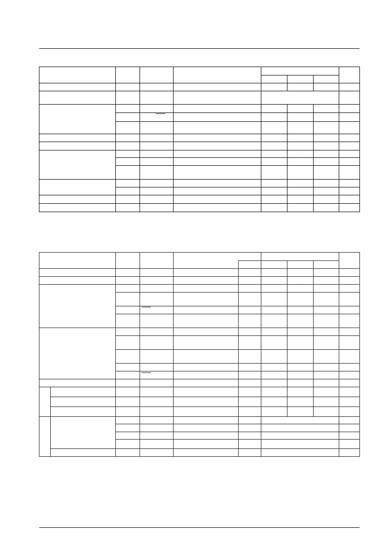
No. 5894-10/14
LC65P29
Parameter
Symbol
Applicable
Conditions
Ratings
Unit
pins/notes
min
typ
max
Maximum supply voltage
V
DD
max
V
O
V
DD
OSC2
–0.3
+7.0
V
Output voltage
Values up to the generated voltage
are allowed.
V
V
I
1
V
I
2
OSC1
*
1
–0.3
V
DD
+ 0.3
V
DD
+ 0.3
V
Input voltage
TEST, RES
–0.3
V
V
I
3
Ports with
PE specifications
–0.3
V
DD
+ 0.3
V
I/O voltage
V
IO
I
OP
I
OA
Σ
I
OA
1
PA, PC, PD
–0.3
+15
mA
Peak output current
PA, PC, PD
–2
+20
mA
PA, PC, PD
The 100 ms average per pin
–2
+20
mA
Average output current
PA
The total current for pins PA0 to PA3
*
2
–6
+40
mA
Σ
I
OA
2
PC, PD
The total current for pins PC0 to PC3 and
PD0 to PD3
*
3
–14
+90
mA
Allowable power dissipation
Pdmax1
Ta = –30 to +70°C(DIP24S)
360
mW
Pdmax2
Ta = –30 to +70°C(MFP30S)
150
mW
Operating temperature
Topr
–30
+70
°C
Storage temperature
Tstg
–55
+125
°C
Absolute Maximum Ratings
at Ta = 25°C, V
SS
= 0 V
Parameter
Symbol
Applicable
Conditions
Ratings
Unit
pins/notes
V
DD
[V]
min
typ
max
Operating supply voltage
V
DD
V
ST
V
IH
1
V
DD
V
DD
PA, PC, PD
3.0
6.0
V
Standby supply voltage
RAM and register retention
*
1.8
6.0
V
Output n-channel transistor off
0.7 V
DD
13.5
V
V
IH
2
PE
When the port E input option
is selected
0.7 V
DD
V
DD
V
High-level input voltage
V
IH
3
RES
1.8 to6.0
0.8 V
DD
V
DD
V
V
IH
4
OSC1
When the RC oscillator and
external clock option is selected
0.8 V
DD
V
DD
V
V
IL
1
PA, PC, PD
Output n-channel transistor off
V
SS
0.3 V
DD
V
V
IL
2
PE
When the port E input option
is selected
V
SS
0.3 V
DD
V
Low-level input voltage
V
IL
3
OSC1
When the RC oscillator and
external clock option is selected
V
SS
0.25 V
DD
V
V
IL
4
V
IL
5
TEST
V
SS
V
SS
0.3 V
DD
0.25 V
DD
4330 (0.92)
V
RES
V
Operating frequency (cycle time)
E
G
fop(t
CYC
)
200 (20)
kHz (μs)
Frequency
fext(text)
OSC1
See Figure 1
200 (20)
4330 (0.92)
kHz (μs)
Pulse width
textH, textL
OSC1
See Figure 1
69
ns
Rise and fall times
textR, textF
OSC1
See Figure 1
50
ns
Cext
OSC1, OSC2
See Figure 2
4 to 6
220 ±5%
pF
Two-pin RC oscillator
Cext
OSC1, OSC2
See Figure 2
220 ±5%
pF
k
k
Rext
OSC1, OSC2
See Figure 2
4 to 6
6.8 ±1%
Rext
OSC1, OSC2
See Figure 2
15.0 ±1%
Ceramic oscillator
See Figure 2
See Table 1
Allowable Operating Conditions
at Ta = –30 to +70°C, V
SS
= 0 V, V
DD
= 3.0 to 6.0 V
Notes: 1. Values up to the generated oscillator amplitude are allowed when driven internally using the guaranteed circuit constant values with the oscillator
circuit shown in figure 2.
2. The average over a 100 ms period.
Note
*
: Applications must maintain the operating supply voltage (V
DD
) until the IC has entered the standby state when a HALT instruction is executed.
Also, applications must assure that chattering (key bounce) noise is not input to the PA3 pin during a HALT instruction execution cycle.
c
c
相關PDF資料 |
PDF描述 |
|---|---|
| LC65F1306A* | |
| LC65F1306A | 4-Bit Single-Chip CMOS Microcontroller for Small-Scale Control Applications |
| LC65P1104 | On-Chip UVEPROM 4-Bit Single-Chip Microcontroller |
| LC662106A | Four-Bit Single-Chip Microcontrollers with 4, 6, and 8 KB of On-Chip ROM |
| LC662306A | Four-Bit Single-Chip Microcontrollers with 6 KB of On-Chip ROM(4位單片微控制器(帶6K字節(jié)片上ROM)) |
相關代理商/技術參數(shù) |
參數(shù)描述 |
|---|---|
| LC65F1306A | 制造商:SANYO 制造商全稱:Sanyo Semicon Device 功能描述:4-Bit Single-Chip CMOS Microcontroller for Small-Scale Control Applications |
| LC65P0101 | 制造商:未知廠家 制造商全稱:未知廠家 功能描述:Microcontroller |
| LC65P1104 | 制造商:SANYO 制造商全稱:Sanyo Semicon Device 功能描述:One-Time Programmable 4-Bit Single-Chip Microcontroller |
| LC65P29 | 制造商:SANYO 制造商全稱:Sanyo Semicon Device 功能描述:One-Time Programmable 4-Bit Single-Chip Microcontroller |
發(fā)布緊急采購,3分鐘左右您將得到回復。