- 您現(xiàn)在的位置:買賣IC網(wǎng) > PDF目錄358736 > LA7337 (Sanyo Electric Co.,Ltd.) SECAM-Format VCR Chroma Signal-Processing Circuit(SECAM格式VCR色度信號處理電路) PDF資料下載
參數(shù)資料
| 型號: | LA7337 |
| 廠商: | Sanyo Electric Co.,Ltd. |
| 英文描述: | SECAM-Format VCR Chroma Signal-Processing Circuit(SECAM格式VCR色度信號處理電路) |
| 中文描述: | SECAM制式格式錄像機(jī)色度信號處理電路(SECAM制式格式錄像機(jī)色度信號處理電路) |
| 文件頁數(shù): | 4/7頁 |
| 文件大小: | 123K |
| 代理商: | LA7337 |
No. 5288-4/7
LA7337
[Record/playback mode settings]
Pin 16 = low
→
record mode
Pin 16 = high
→
playback mode
[Bell filter offset adjustment]
Increasing the pin 6 voltage increases the 1.1-MHz bell filter center frequency (f
0
).
Increasing the pin 5 voltage increases the 4.3-MHz bell filter center frequency (f
0
).
[Test mode settings]
The IC enters test mode if pin 6 is set to 5 V. The pin 5, 11, 17, and 26 outputs behave as follows in this mode.
Pin 5: The 4.43-MHz VCO output appears (However, note that a load of about 1 k
is required between this pin and
V
CC
.)
Pin 11: The 1.1-MHz band-pass filter output appears.
Pin 17: The 4.3-MHz band-pass filter output appears.
Pin 26: The BGP (used for SECAM discrimination, playback AGC, and record killer) can be monitored.
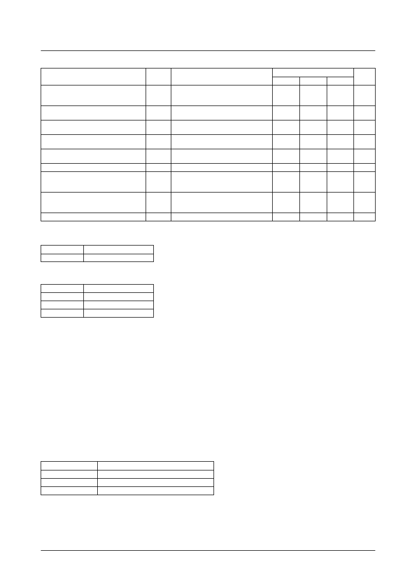
Standard Input Signal Levels
Continued from preceding page.
Parameter
Symbol
Conditions
Ratings
Unit
min
typ
max
Playback mode phase detector output
difference voltage (1)
V5 = V6 = 0 V, SW8B = on, V16 = 5 V,
S27 = composite sync., S13 = sine wave
(50 mVp-p, f = 1.0625/1.1016 MHz)
V
SCPD1
150
180
mV
Playback mode phase detector output
difference voltage (2)
V
SCPD2
As above, except S13 = sine wave
(50 mVp-p, f = 627 kHz)
100
mV
Playback mode SECAM discriminator
characteristics (1)
V
SCMP1
V16 = 5 V, SW23 = SW24 = On
4.5
V
Playback mode SECAM discriminator
characteristics (2)
V
SCMP2
V16 = 5 V, SW23 = SW24 = On
0.5
V
SECAM discriminator comparator
threshold voltage
V
TCOMP
SW25 = On
3.2
3.5
3.8
V
Record/playback control threshold voltage
V
TRP
2.3
2.5
2.7
V
V16 = 0 V, SW25 = on, V25 = 3 V,
S27 = composite sync., S15 = sine wave
(200 mVp-p, f = 4.286 MHz)
Forced SECAM mode threshold voltage
V
THSM
4
V
V16 = 0 V, SW25 = on, V25 = 4 V,
S27 = composite sync., S15 = sine wave
(200 mVp-p, f = 4.286 MHz)
Forced mute mode threshold voltage
V
THMM
1
V
Reference voltage
V
REG
4.1
4.3
4.5
V
REC-IN (pin 15)
The 200 mVp-p ID component
PB-IN (pin 13)
50 mVp-p
Internal filter group delay times (reference values)
1.1 MHz BPF
460 ns (PB) 430 ns (REC)
2.2 MHz BPF
180 ns
4.3 MHz BPFA
230 ns
4.3 MHz BPFB
170 ns
[Muting control table]
Voltage applied to pin 1
Output signal mode (pins 17 and 11)
4 V or higher
Forced SECAM
Open
AUTO (Uses the output of the internal discriminator)
1 V or lower
Forced mute mode
相關(guān)PDF資料 |
PDF描述 |
|---|---|
| LA7356 | 1K82 OHM 1% 1/3W METAL FILM RESISTOR TH |
| LA7356M | For Use in VCR Products PAL/SECAM (MESECAM) Discrimination IC |
| LA7357 | PAL/SECAM Discrimination Circuit for VHS VCRs(用于VHS VCR的PAL/SECAM的鑒別電路) |
| LA7358M | Monolithic Linear IC For VCR SECAM Chroma Signal Processor |
| LA7371A | RECORDING AND PLAYBACK AMPLIFIER FOR VHS VIDEO RECORDERS |
相關(guān)代理商/技術(shù)參數(shù) |
參數(shù)描述 |
|---|---|
| LA733P | 制造商:ON Semiconductor 功能描述: |
| LA733P WAF | 制造商:ON Semiconductor 功能描述: |
| LA733P/D | 制造商:未知廠家 制造商全稱:未知廠家 功能描述:Amplifier Transistors |
| LA733PRLRP | 制造商:ON Semiconductor 功能描述: |
| LA733Q | 制造商:ONSEMI 制造商全稱:ON Semiconductor 功能描述:Amplifier Transistors (PNP Silicon) |
發(fā)布緊急采購,3分鐘左右您將得到回復(fù)。